

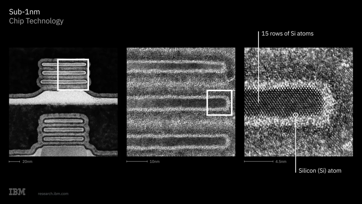
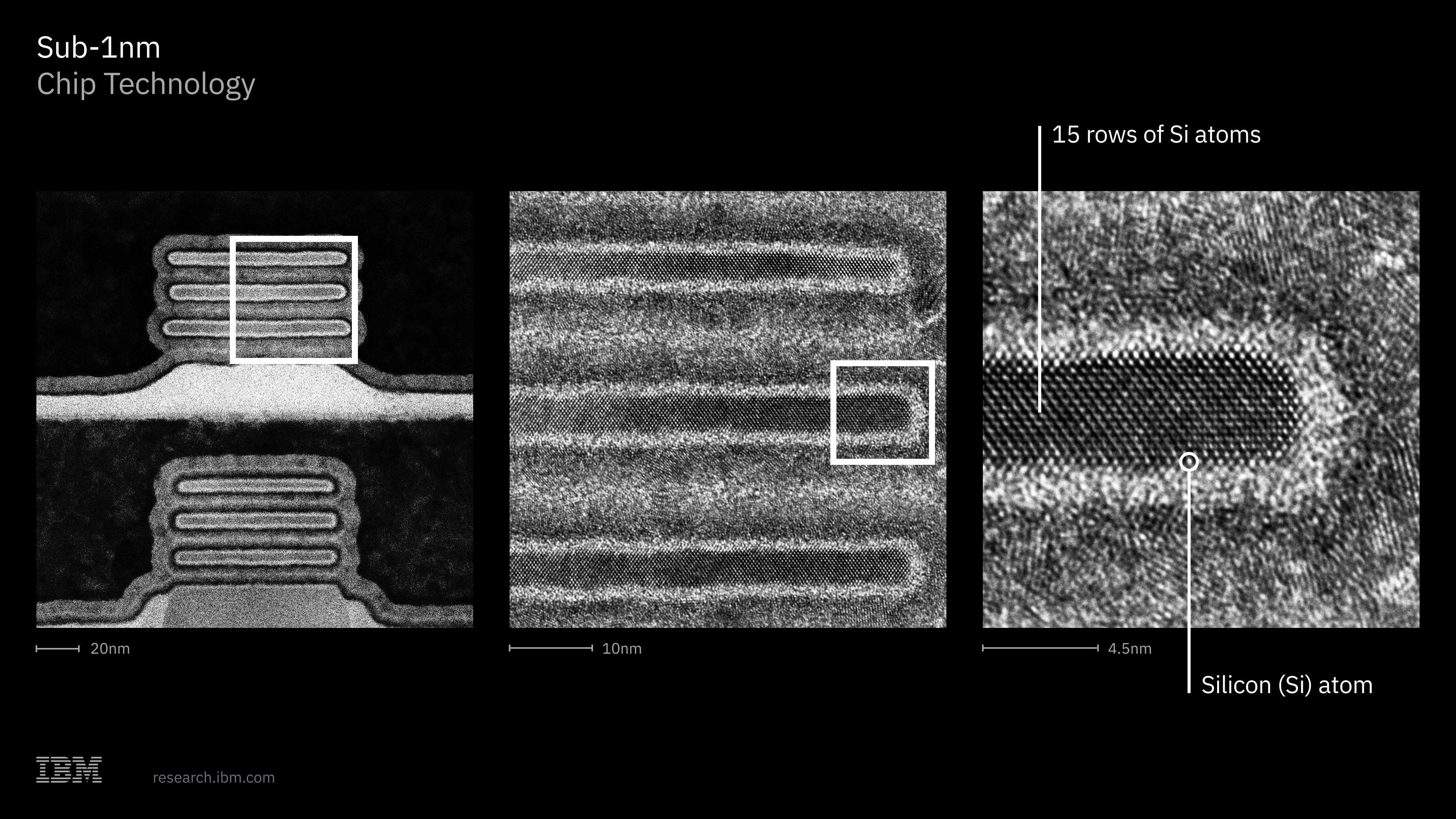
The relentless march of semiconductor advancement has hit a milestone that once belonged strictly to the realm of theoretical physics. IBM has officially unveiled the world’s first sub-1 nanometer (nm) chip technology, a 0.7 nm—or 7 angstrom—node that promises to redefine the limits of transistor density. As the industry grapples with skyrocketing production costs and the slowing cadence of traditional Moore’s Law, this announcement arrives at a pivotal, if not anxiety-inducing, moment for the global tech landscape.
The State of the Industry: A Costly Arms Race
Current high-end graphics processors from industry titans like AMD and Nvidia are largely built on 4 nm-class lithography provided by the Taiwan Semiconductor Manufacturing Company (TSMC). These chips represent the current pinnacle of commercial efficiency, yet they come with a heavy price tag. As the complexity of chip design increases, the cost of manufacturing them follows a steep upward trajectory.
Recently, TSMC hinted at the necessity of increasing the prices charged to chip designers, citing the massive capital expenditure required to maintain the bleeding edge of fabrication. In this climate, IBM’s revelation of a 0.7 nm node is both a beacon of engineering brilliance and a reminder of the mounting economic hurdles facing the next generation of hardware.
Chronology: The Evolution Toward Atomic Scaling
To understand the significance of IBM’s latest achievement, one must look at the historical trajectory of semiconductor scaling.
- The Early Era: Decades ago, "node" names actually corresponded to the physical dimensions of the gate length of a transistor. As we moved from the 90 nm era into the 20 nm era, these names remained relatively grounded in physical reality.
- The Disconnect: As scaling hit physical barriers, the industry pivoted. Names like "7 nm" or "5 nm" ceased to be literal measurements of a specific part of the transistor and became marketing labels denoting a specific generation of density and performance improvements.
- The Modern Arms Race: Today, we see TSMC’s N3 (3 nm) node in high-end smartphones and laptops, while Intel has aggressively pushed its 18A (1.8 nm) process. Analysts largely view these competing nodes as comparable in density, even if their naming conventions diverge.
- The 0.7 nm Milestone: IBM’s announcement marks a departure from the current commercial race. By moving to a 7-angstrom node, IBM is not merely shrinking existing designs but fundamentally altering the geometry of the transistor itself.
The "Nanostack" Architecture: A 3D Revolution
The core of IBM’s breakthrough is the "Nanostack" architecture. To achieve a 0.7 nm node, simply shrinking existing designs is insufficient; the industry has reached a point where electron tunneling and quantum effects make standard 2D scaling unreliable.
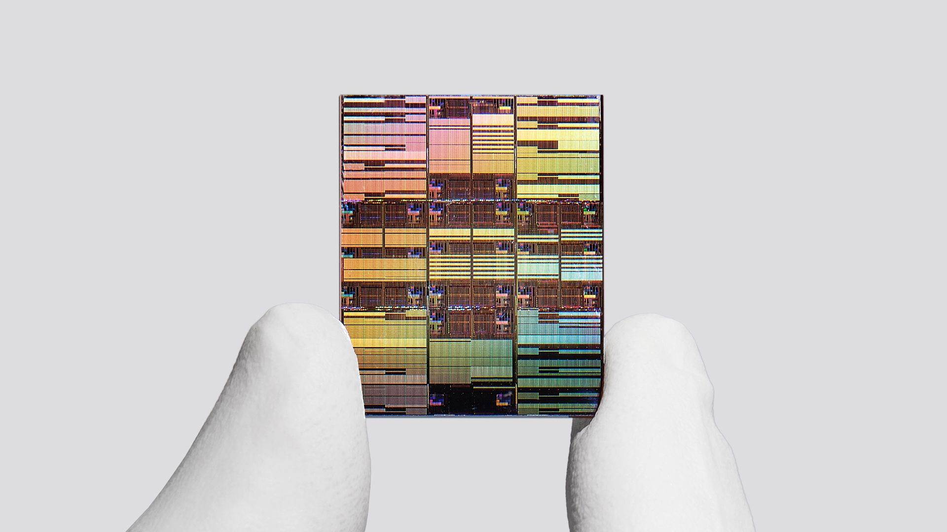
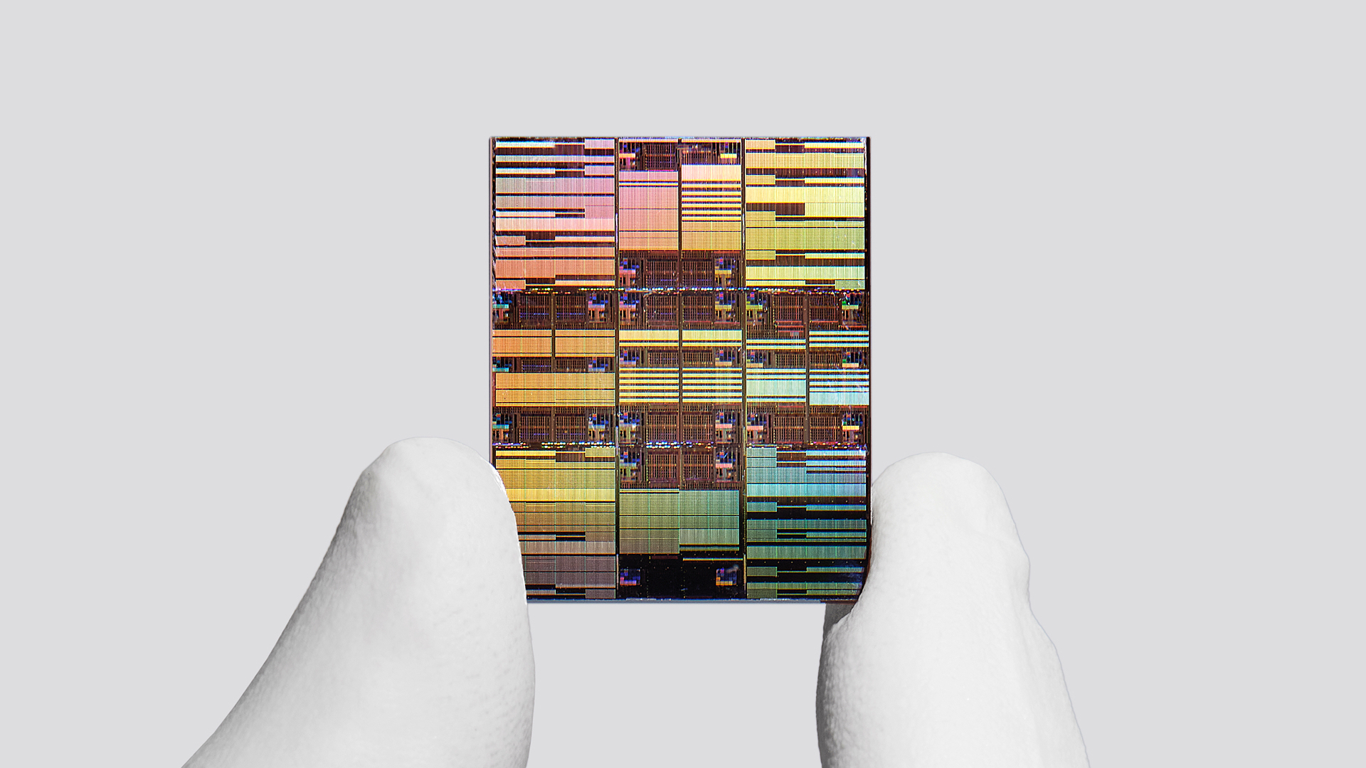
IBM’s Nanostack is the industry’s first three-dimensional, nanosheet-based design. While current "nanosheet" technology (also pioneered by IBM) allows for improved control over current flow, Nanostack takes this a step further by vertically stacking and staggering transistors. This 3D sequential integration allows for a significantly higher density of transistors—nearly 100 billion on a chip the size of a human fingernail.
The beauty of the Nanostack design lies in its flexibility. Because the transistors are stacked vertically, engineers can utilize different material combinations within each layer. This allows for the optimization of power efficiency and performance for each individual transistor, independent of its neighbors. It is, in effect, a custom-tailored environment for every component on the die.
Supporting Data and Technical Reality
It is crucial to approach these claims with a healthy dose of technical skepticism. Industry observers have long noted that "node" labels have become untethered from physical reality. When comparing Intel’s 18A to TSMC’s N3 or the upcoming N2, analysts look at transistor density—the number of transistors per square millimeter—rather than the nanometer designation.
By these metrics, Intel’s 18A and TSMC’s N3 are roughly equivalent, despite the numerical disparity. IBM’s 0.7 nm node claims to break through this barrier by shifting the paradigm from surface area to volume. By building upward, IBM bypasses the "footprint" limitation that has plagued traditional silicon lithography. However, the practical yield of such a complex, 3D-stacked process remains unproven in a high-volume manufacturing environment.
Official Stances and Industry Perspectives
While IBM has been vocal about the technical success of the research, the silence from major foundry partners—TSMC, Samsung, and Intel—is telling. For these companies, the challenge is not just "can we make it," but "can we make it at a price that isn’t prohibitive for consumers?"
Industry experts point out that Moore’s Law was never just about how many transistors could fit on a chip; it was about the economic viability of that density. As fabrication plants—or "fabs"—cost upwards of $20 billion to construct, the cost per transistor is no longer falling as rapidly as it once did. If IBM’s Nanostack requires even more exotic materials or more complex manufacturing steps, the resulting chips could be relegated to ultra-high-end enterprise, AI, or government applications, leaving the consumer market behind.
Implications: The Road Ahead
The implications of IBM’s 0.7 nm technology are profound:
- AI Acceleration: The massive increase in transistor density is tailor-made for artificial intelligence. AI workloads require high-speed memory access and massive parallel processing; a 100-billion-transistor chip could drastically reduce the energy required for LLM (Large Language Model) inference.
- The Sustainability Challenge: As chips become more complex, the energy required to cool them and the resources required to build them increase. The industry must pivot toward efficiency, not just raw power. IBM’s ability to optimize each layer of the Nanostack independently could be a key tool in this fight.
- Economic Stratification: We may be approaching a bifurcation in technology. We could see "commodity" silicon (built on older, cheaper nodes) and "super-compute" silicon (built on cutting-edge 0.7 nm or smaller nodes). This would widen the gap between high-end hardware and entry-level devices.
- Quantum and Beyond: We are rapidly approaching the limit where transistors consist of only a handful of atoms. At the 0.7 nm scale, we are already interacting with the quantum properties of matter. IBM’s research serves as a bridge, preparing the industry for the eventual transition from classical silicon transistors to quantum or alternative-state computing.
Conclusion: A New Era, or a New Wall?
IBM’s 0.7 nm node is a triumph of human ingenuity, demonstrating that the laws of physics are not necessarily a dead-end, but a challenge to be engineered around. The Nanostack architecture offers a viable path forward for increasing performance without relying on the increasingly difficult game of shrinking surface-level features.
However, the path from a laboratory breakthrough to a consumer desktop or smartphone is long and fraught with economic peril. The ultimate question for the consumer is not whether we can reach 0.7 nm, but whether we can do so in a way that remains affordable. As the cost of leading-edge silicon continues to climb, the industry must ensure that this technological marvel doesn’t become a luxury for the few, but a foundation for the next generation of global progress. For now, we wait to see which foundry will be the first to move the Nanostack from a prototype in an IBM lab to a mass-produced reality in our pockets.

