

SANTA CLARA, CA – [Date of Publication] – AMD has officially pulled back the curtain on its most ambitious artificial intelligence accelerator to date, the Instinct MI455X GPU, alongside the groundbreaking Helios rack-scale architecture. Unveiled at the company’s recent "Advancing AI" event, this new platform represents a concerted effort by AMD to directly challenge Nvidia’s long-held supremacy in the burgeoning AI compute market. With the MI455X and Helios, AMD is not just offering a competitive chip, but a comprehensive, large-scale system designed to integrate 72 GPUs into a single, coherent accelerator, marking its first true contender against Nvidia’s formidable NVL72 rack-scale designs, famously used in the Blackwell and upcoming Rubin generations.
AMD executives lauded the MI455X as "by leaps and bounds the most advanced AI accelerator we’ve ever built." From initial specifications and architectural details, it is clear that AMD is bringing its most competitive product yet to the table, both at the individual chip level and within a rack-scale deployment. This strategic move aims to carve out a significant share of the rapidly expanding market for AI training and inference, where demand for raw compute power and high-bandwidth memory continues to skyrocket.
Main Facts: AMD’s New AI Powerhouse
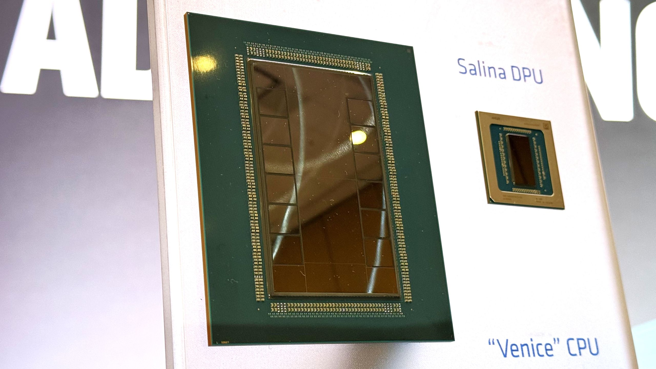
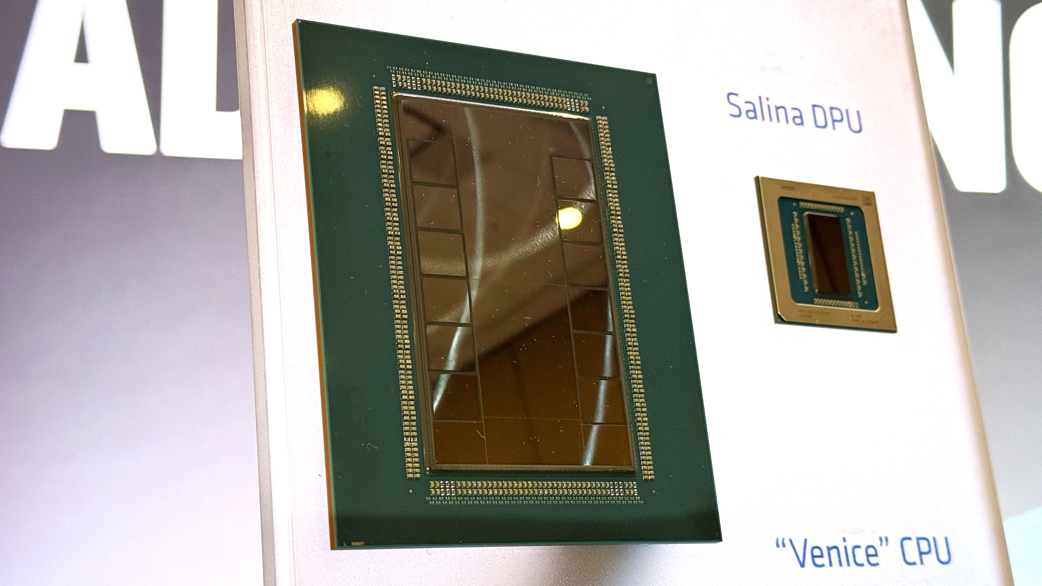
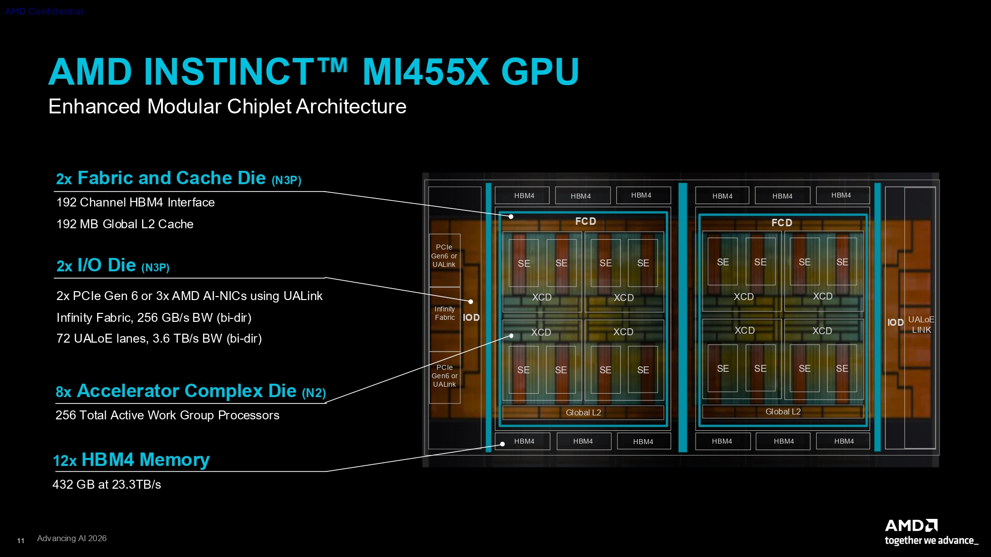
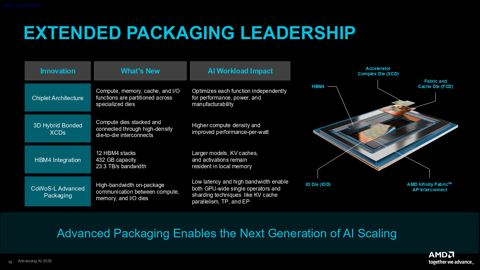
The core of AMD’s latest offering is the Instinct MI455X GPU, a monumental silicon achievement boasting an astonishing 320 billion transistors. This immense transistor count is made possible through sophisticated advanced packaging technologies, a testament to AMD’s prowess in chiplet design. The MI455X integrates four Accelerator Complex Dies (XCDs) stacked atop each Fabric and Cache Die (FCD) using hybrid bonding. These two FCDs are then intricately joined to six stacks of HBM4 memory, two I/O dies, and to each other, leveraging TSMC’s cutting-edge CoWoS-L technology. This multi-die, multi-technology approach allows AMD to optimize each component for its specific role, maximizing performance and efficiency.
A key differentiator in the MI455X’s manufacturing strategy is its heterogeneous use of TSMC’s process technologies. The performance-critical XCDs, which house the primary compute units, are fabricated using the most advanced TSMC 2N gate-all-around (GAA) process technology. This ensures optimal power efficiency and raw computational speed where it matters most. Conversely, the FCDs and I/O dies, which contain elements less dependent on the densest process technologies, are produced on TSMC N3P. This intelligent allocation of manufacturing processes allows AMD to achieve a balance between leading-edge performance and cost-effectiveness.
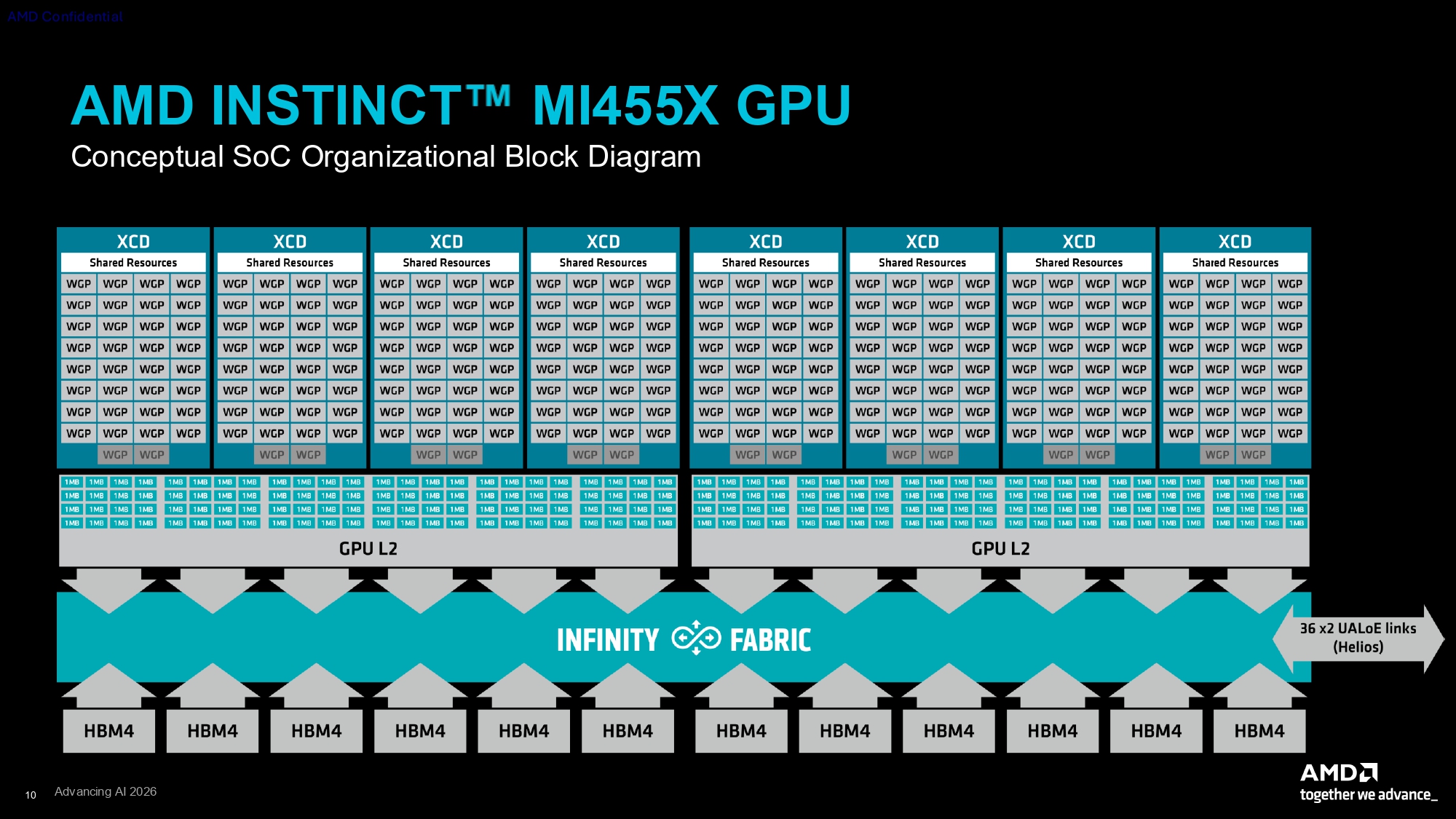
The MI455X is built upon the CDNA 5 architecture, representing a significant evolution from its predecessors. One notable change is the renaming of the fundamental building block within the Accelerator Complex Die from "Compute Unit" to "Work Group Processor" (WGP). While the basic layout of the XCD remains broadly similar, this change signifies a refined approach to workload management and execution. Despite retaining the same number of WGPs as the previous MI355X (256), the CDNA 5 architecture is engineered for a much higher per-WGP throughput, enabling the dramatic performance gains seen in this generation.
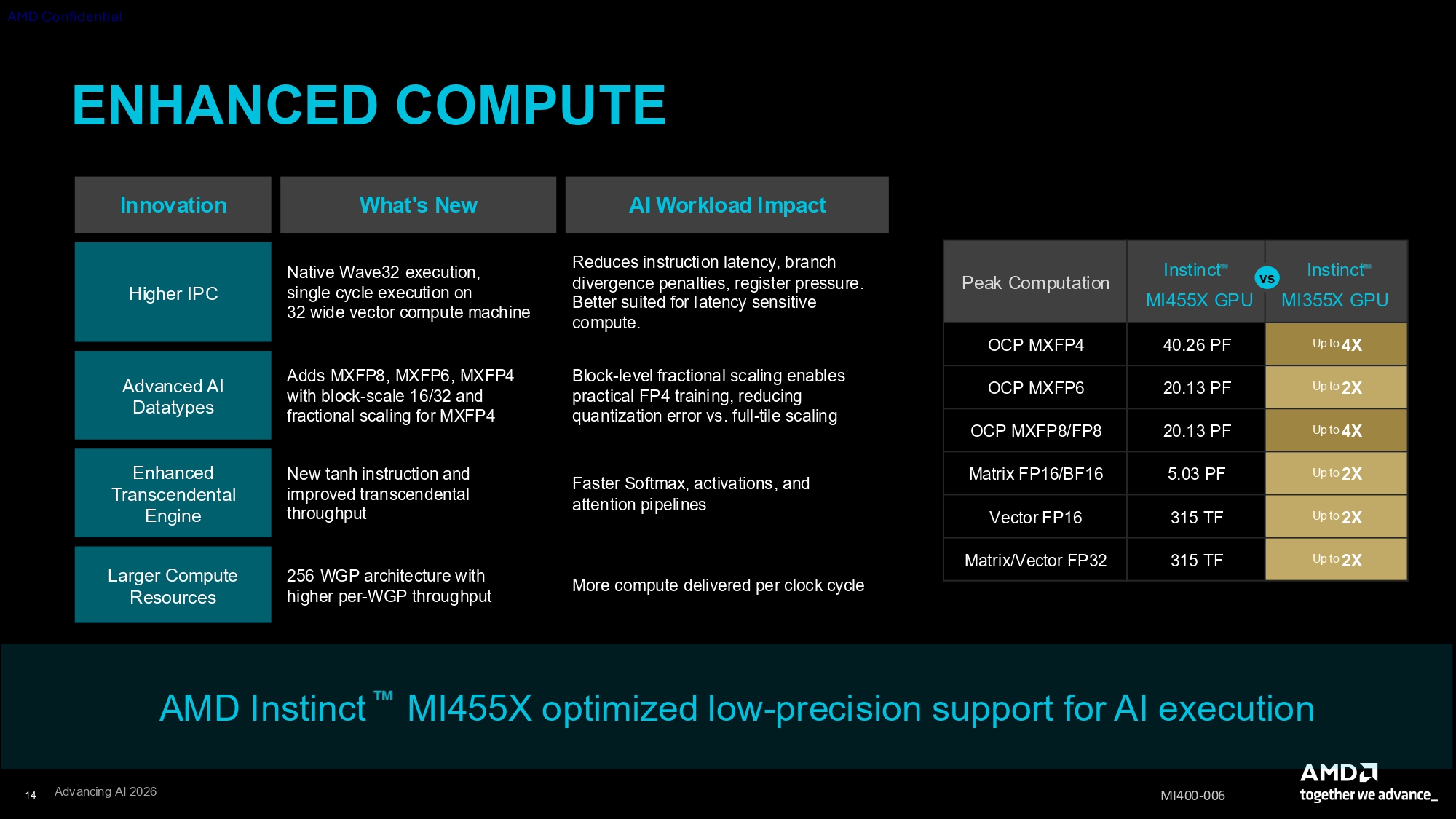
Performance enhancements are particularly pronounced in lower-precision floating-point formats, which are increasingly crucial for AI inference workloads. The MI455X theoretically offers up to 4x faster performance for OCP MXFP8 and MXFP4 formats compared to the CDNA 4 MI355X. Beyond general compute, the CDNA 5 Transcendental Unit has been significantly improved, doubling throughput for essential AI functions like softmax, neural network activations, and attention mechanisms. It also introduces explicit tanh instruction support, vital for various hidden layers within neural networks.
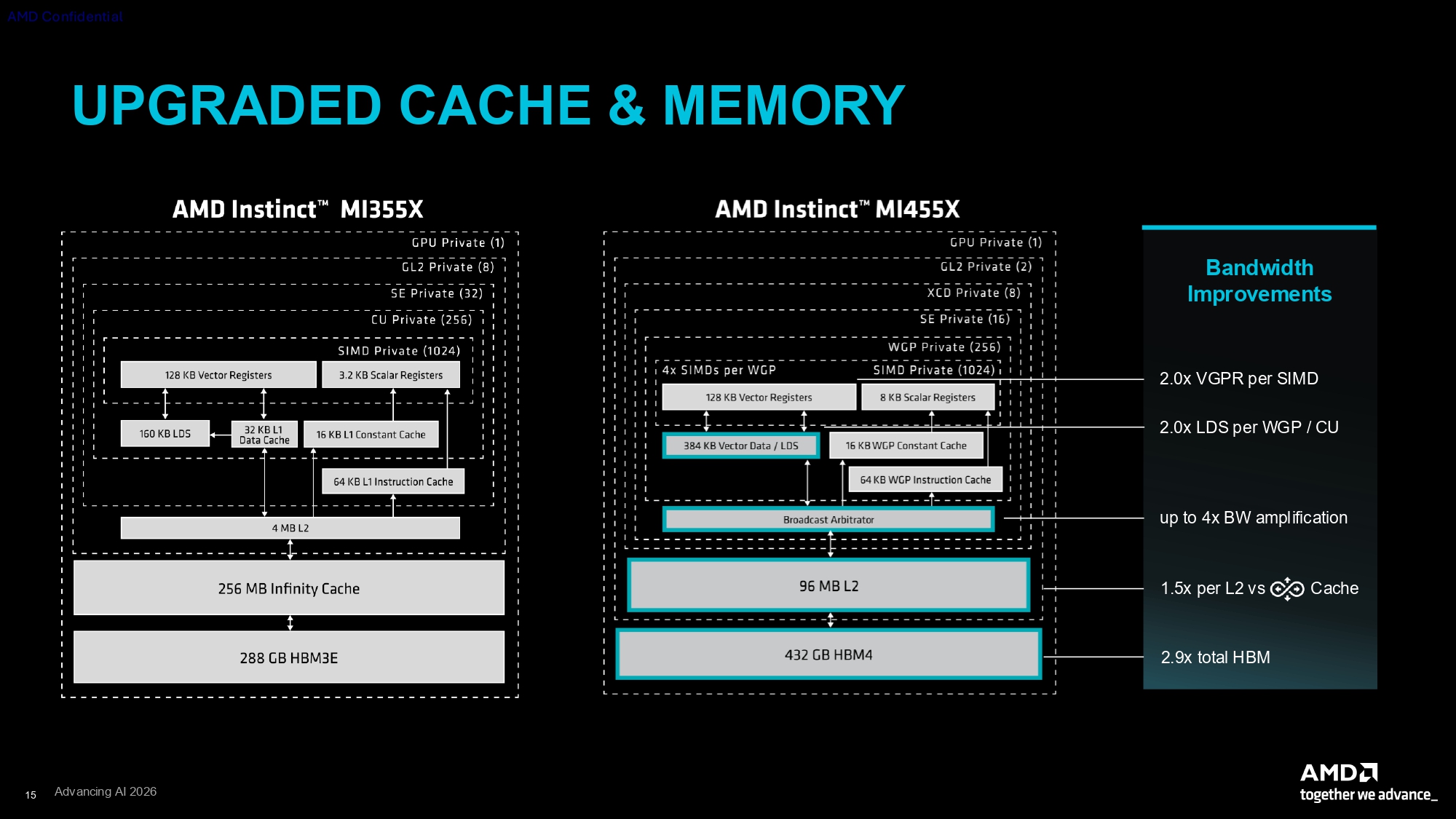
AMD has also undertaken a comprehensive overhaul of the cache and memory hierarchy. The large Infinity Cache found in CDNA 4 has been replaced by a smaller but higher-bandwidth shared L2 cache on each Fabric and Cache Die. Each FCD now features a 96MB L2 slice, totaling 192MB across the chip, a substantial upgrade from the MI355X’s 32MB backed by 256MB Infinity Cache. This new L2 cache configuration reportedly offers 1.5x higher bandwidth per FCD, resulting in a 3x aggregate L2 bandwidth improvement over the MI355X. The Local Data Store (LDS), or scratchpad memory within each WGP, has also doubled to 320 KB, leading to a total of 96MB of LDS across the chip, further enhancing data locality and processing speed.
Critically, the MI455X marks AMD’s transition to HBM4 memory. The GPU incorporates 12 stacks of HBM4 (six per FCD), delivering an impressive 432GB of memory capacity and a staggering 23.3 TB/s of memory bandwidth per GPU. This high memory capacity and bandwidth are paramount for accommodating the ever-growing size of AI models and their associated weights and KV caches, keeping them as close to the GPU as possible for optimal performance. This HBM implementation provides a significant competitive advantage over Nvidia’s initial Rubin GPU, which offers 288GB of HBM4 with up to 22 TB/s of bandwidth. At the rack scale, the MI455X’s HBM advantage translates into 31.1 TB of aggregate HBM across 72 GPUs in the Helios system, a 50% increase over Vera Rubin’s 20.7 TB.
The Helios rack-scale architecture is designed to integrate these 72 MI455X GPUs into a single, coherent memory domain, directly challenging Nvidia’s NVL72 design. This coherent domain ensures that all GPUs can efficiently access and share data, minimizing latency and maximizing throughput for large-scale AI workloads. This holistic approach, combining powerful individual GPUs with a robust interconnect architecture, is translating into tangible business success, with AMD announcing pivotal deals with major industry players like Microsoft and Anthropic.
Chronology: AMD’s Ascent in the AI Arena
AMD’s journey to becoming a formidable player in the AI hardware market has been a strategic, multi-year endeavor. For years, Nvidia has enjoyed near-uncontested dominance in the AI compute space, largely thanks to its CUDA software platform and early lead in GPU acceleration for machine learning. AMD’s previous generations of Instinct accelerators, while technically capable, often struggled to gain significant market traction against Nvidia’s established ecosystem.
The "Advancing AI event this week" serves as a pivotal moment, showcasing the culmination of AMD’s sustained investment in AI R&D. The company’s CDNA architecture, specifically designed for data center compute, has been steadily evolving. The CDNA 4 generation, embodied by the MI355X, laid important groundwork, but the MI455X and CDNA 5 represent a quantum leap. This latest reveal places AMD in a direct, head-to-head competition with Nvidia’s current Blackwell generation and its upcoming Rubin series, which Nvidia has already begun detailing.
The development of the Helios rack-scale architecture is particularly significant. For AMD to truly compete at the hyperscale level, it needed to offer not just powerful individual accelerators, but also a scalable, integrated system that could rival Nvidia’s NVLink-powered multi-GPU designs like NVL72. The Helios platform, with its ability to unify 72 MI455X GPUs into a coherent domain, is AMD’s definitive answer to this challenge. This architectural maturity demonstrates AMD’s commitment to providing end-to-end solutions for the most demanding AI workloads.
The announcement of key customer wins with Microsoft and Anthropic underscores the growing confidence in AMD’s AI capabilities. These partnerships are crucial, not only for revenue but also for validating AMD’s technology in real-world, large-scale deployments, which in turn fuels further development and ecosystem growth. The second half of this year is anticipated to be a critical period, as both Nvidia and AMD begin delivering their next-generation AI products to customers, intensifying the competitive landscape and shaping the future of AI infrastructure.
Supporting Data: A Deep Dive into MI455X Innovations
Architectural Deep Dive
The AMD Instinct MI455X GPU is an engineering marvel, comprising 320 billion transistors packed into a multi-chiplet design. This intricate construction leverages advanced packaging techniques to achieve unprecedented levels of integration and performance. At its core, the MI455X features four Accelerator Complex Dies (XCDs) that are vertically stacked onto two Fabric and Cache Dies (FCDs) using state-of-the-art hybrid bonding technology. Hybrid bonding allows for extremely dense interconnections between the stacked dies, enabling high-bandwidth communication and minimizing latency.
The two FCDs, acting as central hubs, are interconnected and further linked to 12 stacks of HBM4 memory (six stacks per FCD) and two I/O dies. This entire assembly is integrated onto a single package utilizing TSMC’s CoWoS-L (Chip-on-Wafer-on-Substrate with Large reticle) technology. CoWoS-L is a crucial enabler for such complex designs, providing a high-density interposer that facilitates ultra-high bandwidth connections between various chiplets and HBM stacks. This level of integration is essential for managing the vast amounts of data required by modern AI models.
The decision to use heterogeneous process technologies further highlights AMD’s sophisticated approach. The XCDs, containing the primary computational engines, benefit most from the latest process nodes. By fabricating them on TSMC’s 2N Gate-All-Around (GAA) process, AMD achieves superior power efficiency and higher clock speeds, directly translating into increased raw compute performance. In contrast, the FCDs and I/O dies, which manage data fabric and external connectivity, are manufactured on TSMC N3P. This node is still highly advanced but offers a more balanced cost-performance profile for components that don’t require the absolute bleeding edge of transistor density. This selective application of process technologies optimizes the overall chip for both performance and manufacturing cost.
The CDNA 5 architecture introduces a semantic shift in its fundamental compute block, moving from "Compute Unit" to "Work Group Processor" (WGP). While the MI455X maintains 256 WGPs, the same count as the MI355X, the per-WGP throughput has been dramatically increased. This means each WGP in the MI455X can execute more operations per clock cycle, contributing to the overall performance boost without simply scaling up the number of physical compute units.
A significant architectural change in CDNA 5 is the reduction of the wavefront width from 64 to 32. A wavefront represents a group of work items or threads processed concurrently by a workgroup processor. AMD explains that this narrower wavefront size offers several advantages: improved instruction latency, reduced branch divergence penalties (where different threads in a wavefront take different execution paths), and lower register pressure. Furthermore, a 32-wide approach enhances the architecture’s flexibility for interacting with diverse tensor tile sizes and more efficiently mapping compute kernels to the hardware. This aligns the Instinct GPU’s programming model more closely with AMD’s RDNA GPUs, which have utilized a native 32-wide wavefront since their inception, potentially simplifying software development across AMD’s product lines.
Performance Metrics
The CDNA 5 architecture in the MI455X delivers substantial compute performance enhancements over CDNA 4, theoretically doubling and in some cases even quadrupling the peak FLOPS (Floating Point Operations Per Second) achievable from the chip. This generational leap is particularly impactful for lower-precision floating-point formats, which are critical for accelerating AI inference workloads where precision requirements can be relaxed to gain speed and efficiency. The OCP MXFP8 and MXFP4 formats, for instance, are quoted as being up to 4X faster on the MI455X compared to the CDNA 4 MI355X.
Let’s examine the theoretical peak FLOPS comparisons:
| Metric | Instinct MI355X | Instinct MI455X | Nvidia Rubin |
|---|---|---|---|
| NVFP4 (dense) | — | — | 35 PF |
| OCP MXFP4 | 10 PF | 40.26 PF | — |
| OCP MXFP6 | 10 PF | 20.13 PF | 17.5 PF |
| OCP MXFP8 | 10 PF | 20.13 PF | 17.5 PF |
| Matrix FP16/BF16 | 2.5 PF | 5.03 PF | 4 PF |
| Vector FP16 | 157.3 TF | 315 TF | — |
| Matrix FP32 | 157.3 TF | 315 TF | 400 TF |
| Vector FP32 | 157.3 TF | 315 TF | 130 TF |
PF = PetaFLOPS (10^15 FLOPS), TF = TeraFLOPS (10^12 FLOPS)
This table clearly illustrates the MI455X’s impressive theoretical gains, especially in mixed-precision formats vital for AI. The 40.26 PF in OCP MXFP4 and 20.13 PF in OCP MXFP8 highlight a significant advantage over Nvidia’s Rubin in these specific formats. Even in Matrix FP16/BF16, the MI455X at 5.03 PF theoretically surpasses Rubin’s 4 PF. While Rubin shows higher Matrix FP32 performance, the MI455X doubles its Vector FP32 performance compared to its predecessor and significantly outperforms Rubin in this specific vector computation.
However, AMD itself offered a pragmatic caveat: "we’d be careful about drawing too many conclusions from these head-to-head peak FLOPS numbers, as the realized performance of these GPUs in the real world is likely to be much lower in practice." This transparency is crucial, emphasizing that theoretical peaks are aspirational, and the actual performance heavily depends on software optimization and workload characteristics. The ongoing challenge for AMD will be to ensure that its software stack and developer tools enable users to maximize these impressive hardware capabilities.
Beyond general compute, the CDNA 5 Transcendental Unit has received a significant boost. This unit specializes in transcendental math functions, which are fundamental to many AI operations. AMD states that its throughput has doubled compared to CDNA 4, directly impacting the performance of critical functions such as softmax (used in classification layers), neural network activations (like ReLU, sigmoid, etc.), and attention mechanisms (central to transformer models). The addition of an explicit tanh instruction is also notable, as the hyperbolic tangent function is frequently used in hidden layers of neural networks for non-linear transformations. These improvements contribute to more efficient and faster execution of core AI algorithms.
Memory and Interconnect Innovations
The MI455X introduces a profoundly revised cache and memory hierarchy, designed to optimize data flow and minimize latency – critical factors for AI workloads. AMD has moved away from the large Infinity Cache design of CDNA 4. Instead, the MI455X features a smaller but significantly higher-bandwidth shared L2 cache on each Fabric and Cache Die (FCD). Each FCD is equipped with a 96MB L2 slice, resulting in a total of 192MB of L2 cache across the entire GPU. This is a considerable increase from the 32MB L2 cache (backed by 256MB Infinity Cache) on the MI355X. AMD reports that this new L2 cache configuration delivers 1.5x higher bandwidth per FCD, leading to a remarkable 3x increase in aggregate L2 bandwidth compared to the MI355X. This enhancement ensures that data frequently accessed by the WGPs remains closer to the compute elements, reducing trips to slower main memory.
Further enhancing data locality and throughput, the Local Data Store (LDS), or scratchpad memory within each Work Group Processor (WGP), has been doubled in size to 320 KB per WGP. Across the entire chip, this sums up to 96MB of LDS, twice the capacity of the largest CDNA 4 implementation in the MI355X. The LDS SRAM also offers higher read and write bandwidth per clock than its predecessor, though specific figures were not provided. This increased, faster scratchpad memory is vital for intermediate computations and frequently reused data within a WGP, reducing contention for shared cache resources.
The most critical memory innovation in the MI455X is the adoption of HBM4 (High Bandwidth Memory Generation 4). The GPU features 12 stacks of HBM4, with six stacks connected to each FCD. This configuration provides a massive 432GB of total memory capacity and an astounding 23.3 TB/s of memory bandwidth per GPU. High memory capacity is essential for hosting the massive parameters of large language models (LLMs) and their growing KV (Key-Value) caches during inference. Equally important, the immense bandwidth ensures that these large models can be fed to the GPU’s compute units without bottlenecks, which is crucial for achieving high throughput.
This HBM implementation gives the MI455X a distinct advantage over Nvidia’s recently detailed Rubin GPU in isolation. Nvidia’s initial Rubin configuration offers 288GB of HBM4 with up to 22 TB/s of bandwidth. The MI455X’s 432GB capacity is 1.5 times larger, and its 23.3 TB/s bandwidth is slightly higher. This advantage is amplified at the rack scale: a Helios system with 72 MI455X GPUs boasts an aggregate HBM capacity of 31.1 TB, a staggering 50% more than the 20.7 TB aggregate capacity of a 72-GPU Vera Rubin system. Coupled with the Helios rack-scale architecture’s ability to join all this GPU memory into a single coherent domain, AMD’s advantages in memory capacity and bandwidth are poised to significantly impact AI inference performance, which is heavily reliant on data locality and memory access speeds.
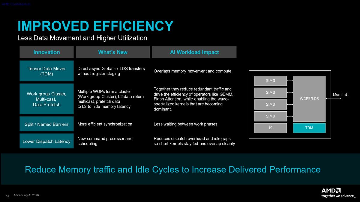
Efficient data movement across the chip is paramount for minimizing power consumption and maximizing performance. The CDNA 5 Tensor Data Mover (TDM) has been significantly improved. Similar to Nvidia’s Tensor Memory Accelerator, the TDM accelerates the generation of tensor-specific memory addresses and facilitates the direct movement of related data from memory without involving the shader engines. In CDNA 5, the TDM gains the crucial ability to move data directly from DRAM to the WGP LDS cache, bypassing intermediate cache levels. This direct path reduces latency and frees up cache resources for other operations.
AMD has also implemented multicast support for memory reads to the WGPs. AI workloads frequently require multiple WGPs to access and operate on the same weights and activations concurrently. By using multicast, a single memory read operation can be broadcast to numerous WGPs simultaneously. This innovation effectively increases memory bandwidth, drastically reduces duplicated traffic on the internal bus, and lowers overall power consumption by avoiding redundant data transfers. While Nvidia has incorporated similar capabilities in its GPUs since the Hopper generation, its inclusion in CDNA 5 underscores AMD’s intense focus on optimizing data movement and efficiency this generation.
Official Responses: AMD’s Strategic Vision and Acknowledgment
AMD’s messaging surrounding the MI455X and Helios architecture has been confident yet grounded. The company’s assertion that the MI455X is "by leaps and bounds the most advanced AI accelerator we’ve ever built" reflects the significant engineering effort and strategic investment poured into this generation. This bold claim is backed by the impressive technical specifications and theoretical performance numbers.
Crucially, AMD also demonstrated a realistic understanding of the complex challenges in AI hardware deployment. During press sessions, the company candidly admitted that "the realized performance of these GPUs in the real world is likely to be much lower in practice" than the theoretical peak FLOPS. This acknowledgment highlights the critical role of software optimization, driver maturity, and application-specific tuning in unlocking the full potential of high-performance AI hardware. It signals that AMD is aware of the journey ahead in building out its ROCm software ecosystem to rival Nvidia’s well-established CUDA platform.
The announcement of "pivotal deals with Microsoft and Anthropic" serves as powerful validation for AMD’s new AI platform. Microsoft, a titan in cloud computing and AI services, and Anthropic, a leading AI safety and research company known for its Claude LLM, are significant customers whose adoption of MI455X accelerators will provide invaluable real-world feedback and accelerate the platform’s optimization. These partnerships are not merely sales but strategic collaborations that will help AMD refine its hardware and software, broaden its ecosystem, and establish credibility in the fiercely competitive AI market.
Implications: Reshaping the AI Landscape
Reshaping the AI Landscape
The introduction of the AMD Instinct MI455X GPU and the Helios rack-scale architecture marks a pivotal moment in the AI hardware industry. This generation positions AMD as a truly formidable challenger to Nvidia’s long-standing, near-monopolistic dominance in AI compute. For years, Nvidia’s NVLink interconnect and unified memory architectures, culminating in systems like NVL72, have been unmatched in their ability to scale AI workloads across multiple GPUs. Helios, with its 72-accelerator scale-up domain and coherent memory, is AMD’s first direct and compelling answer to this, finally offering hyperscalers and large enterprises a viable alternative for massive AI training and inference tasks.
This intensified competition is beneficial for the entire AI ecosystem. Customers will have more choice, potentially leading to better pricing, accelerated innovation, and more diverse architectural approaches. AMD’s competitive HBM4 capacity (432GB per GPU, 31.1 TB per rack) and bandwidth advantages over Nvidia’s Rubin could be a major draw for workloads involving extremely large models or those sensitive to memory access patterns. As AI models continue to grow in size and complexity, the ability to keep more parameters and data on-device and accessible at high speeds becomes increasingly critical.
Software Optimization Challenge
Despite the impressive hardware specifications and theoretical performance figures, AMD faces the ongoing and significant challenge of software optimization. The gap between theoretical peak FLOPS and realized performance in real-world applications is often substantial, as AMD itself acknowledged. Nvidia’s decades-long investment in its CUDA ecosystem, developer tools, libraries, and community support has created a powerful moat.
For the MI455X and Helios to truly succeed, AMD must aggressively expand and mature its ROCm software platform. This involves ensuring robust compiler support, optimizing AI frameworks (like PyTorch and TensorFlow) for CDNA 5, providing efficient libraries for common AI operations, and fostering a vibrant developer community. Customer wins with Microsoft and Anthropic are crucial here, as their engineers will contribute to testing, optimizing, and providing feedback, accelerating ROCm’s development and adoption. The performance of the hardware is only as good as the software that can harness it, and AMD’s success in this area will be critical to translating its hardware prowess into market share.
Future Outlook
The second half of this year is poised to witness an unprecedented heating up of the race for AI compute superiority. As both Nvidia and AMD begin delivering their next-generation products, the market will gain a clearer picture of their relative strengths and weaknesses in real-world deployments. This heightened competition promises to drive further innovation, pushing the boundaries of what’s possible in AI hardware and software.
AMD’s long-term vision positions it as a key enabler across the entire spectrum of AI, from cloud data centers to enterprise and edge computing. The MI455X and Helios architecture are foundational elements of this strategy, demonstrating AMD’s capability to deliver top-tier performance for the most demanding AI workloads. As AI continues to permeate every industry, the availability of diverse, high-performance, and scalable compute options from multiple vendors will be crucial for democratizing access to advanced AI capabilities and accelerating global technological progress. The market awaits with anticipation to see how these powerful new platforms will transform the landscape of artificial intelligence.

