

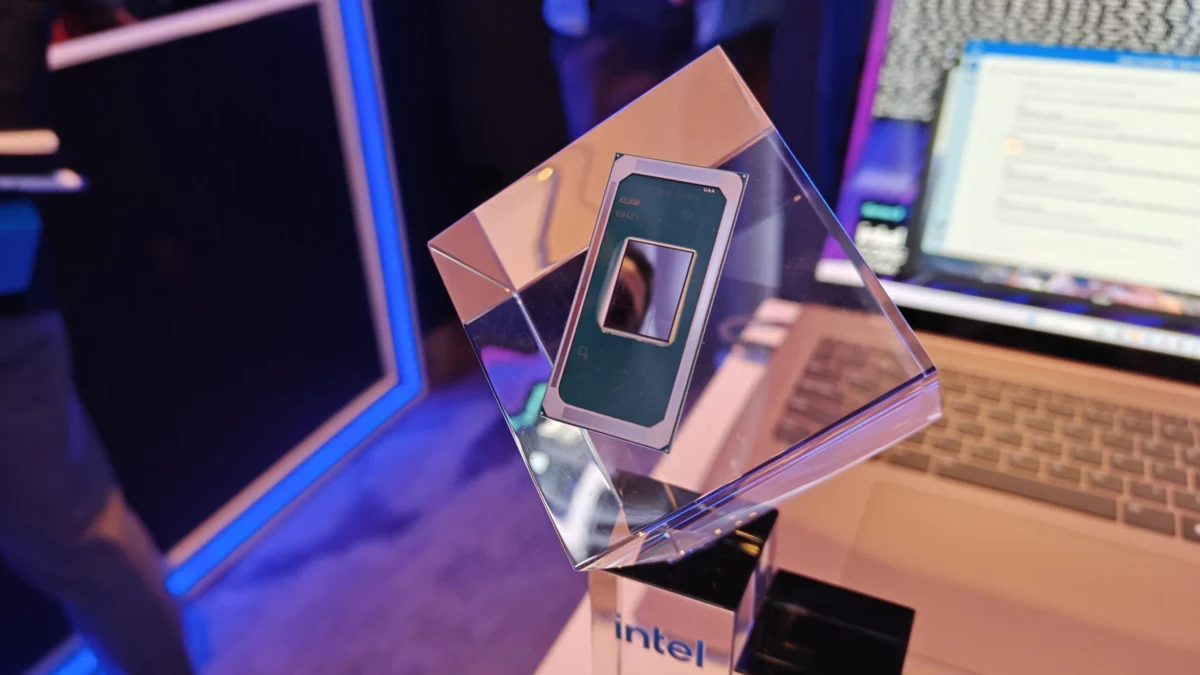
Santa Clara, CA – Intel has officially announced that its performance-optimized 18A-P process node has entered risk production, marking a pivotal step toward its high-volume manufacturing. Revealed at VLSI 2026, this enhanced version of the foundational 18A node is set to power future generations of Intel’s cutting-edge products, including the highly anticipated Panther Lake client CPUs and Xeon 6+ data center processors. The company touts impressive gains, including a 9% improvement in performance at the same power level, or an 18% reduction in power consumption for equivalent performance, along with significant advancements in transistor design, thermal management, and interconnect efficiency.
This announcement underscores Intel’s aggressive roadmap to reclaim process leadership, reinforcing its "five nodes in four years" strategy. The transition to risk production signals a growing confidence in the maturity and capabilities of its most advanced manufacturing technology, not only for internal products but also for its burgeoning Intel Foundry Services (IFS) division, which seeks to attract major external clients.
Main Facts
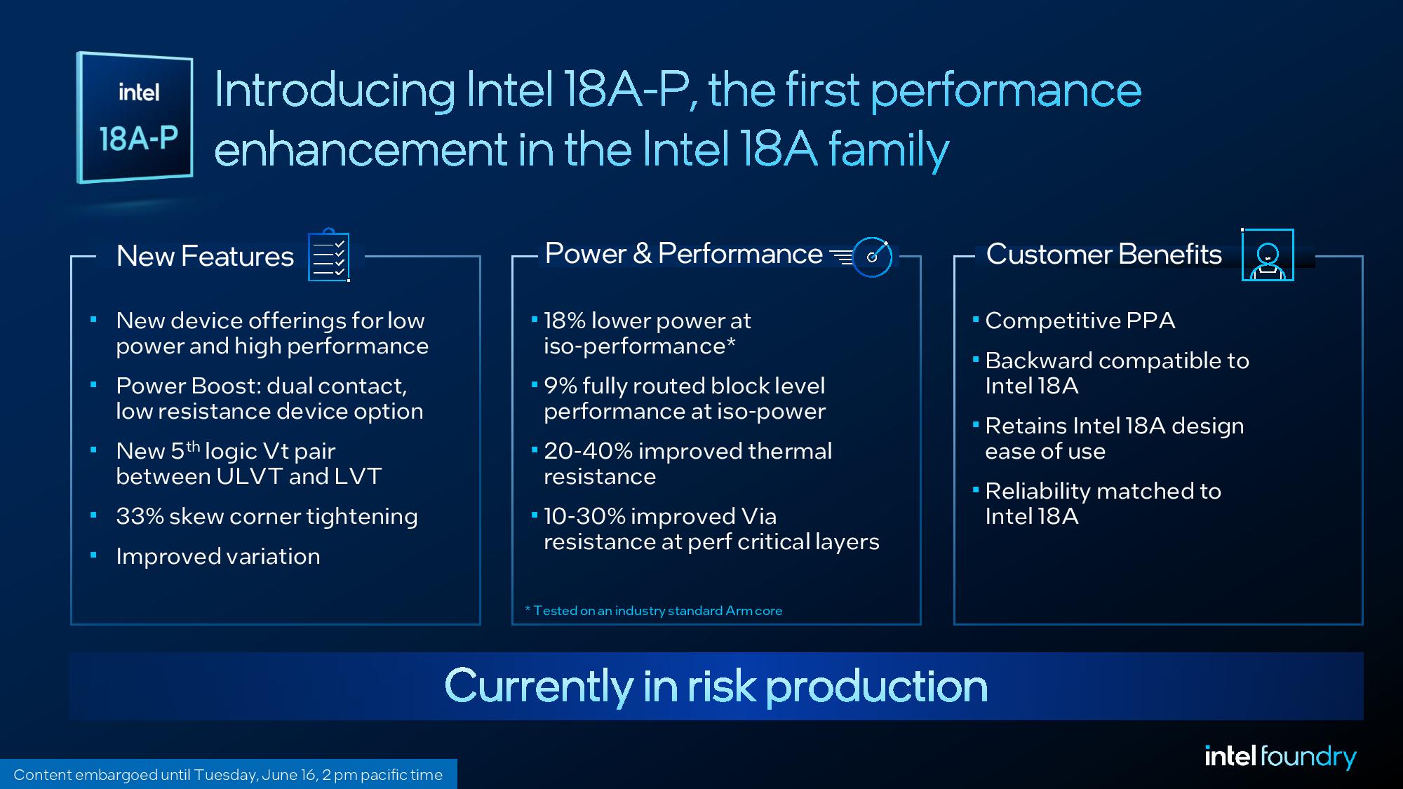
Intel’s 18A-P represents a critical evolution in semiconductor manufacturing, building upon the innovations introduced with the 18A process. The key takeaway from the VLSI 2026 presentation is the tangible performance and power efficiency benefits it offers. Specifically, Intel has demonstrated a 9% increase in frequency at the same operating power, or an 18% decrease in power consumption at the same frequency, particularly at a reference voltage of 0.75 volts. These figures are derived from testing on a standard Arm core subblock, indicating real-world applicability to processor designs.
The term "risk production" is a significant milestone in semiconductor fabrication. It signifies a low-volume manufacturing phase where Intel will produce full wafers of 18A-P on its standard production lines. Unlike experimental or pilot runs, risk production uses the actual tools and processes intended for mass production, albeit with a limited scope. The primary goal at this stage is to meticulously gather data on critical parameters such as defect rates, performance consistency, and variability across wafers. This data is indispensable for fine-tuning the manufacturing process, identifying potential bottlenecks, and ensuring robust yields before transitioning to high-volume mass production. While a typical new node might see a 12 to 24-month gap between risk and mass production, 18A-P, being an optimized revision rather than an entirely new node, is expected to have a tighter timeline.
Crucially, 18A-P is designed to be backward compatible with existing 18A designs. This means that chip designers can port their 18A-based layouts to the 18A-P process without requiring extensive redesigns. While opting for new transistor options available with 18A-P might necessitate some design adjustments to fully leverage the maximum benefits, the fundamental compatibility ensures a smoother transition for early adopters and allows for incremental performance gains even without significant modifications. This flexibility is vital for accelerating product development cycles and minimizing design costs.
Among the specific products slated to benefit from 18A-P are Intel’s next-generation client CPUs, codenamed Panther Lake, and advanced data center processors, Xeon 6+. These products are expected to leverage the enhanced performance, reduced power consumption, and improved thermal characteristics to deliver superior computing experiences across consumer and enterprise segments.
A Journey Through Innovation: The Chronology of Intel’s 18A and 18A-P Development
Intel’s current trajectory in process technology is a direct outcome of its strategic pivot, announced several years ago, to accelerate its manufacturing roadmap and regain its long-held leadership position. This ambitious plan, famously dubbed "five nodes in four years," aimed to rapidly advance through several critical process generations: Intel 7, Intel 4, Intel 3, Intel 20A, and finally, Intel 18A. Each node represents a significant leap in transistor density, performance, and power efficiency, with 18A being positioned as the ultimate frontier in this aggressive push.
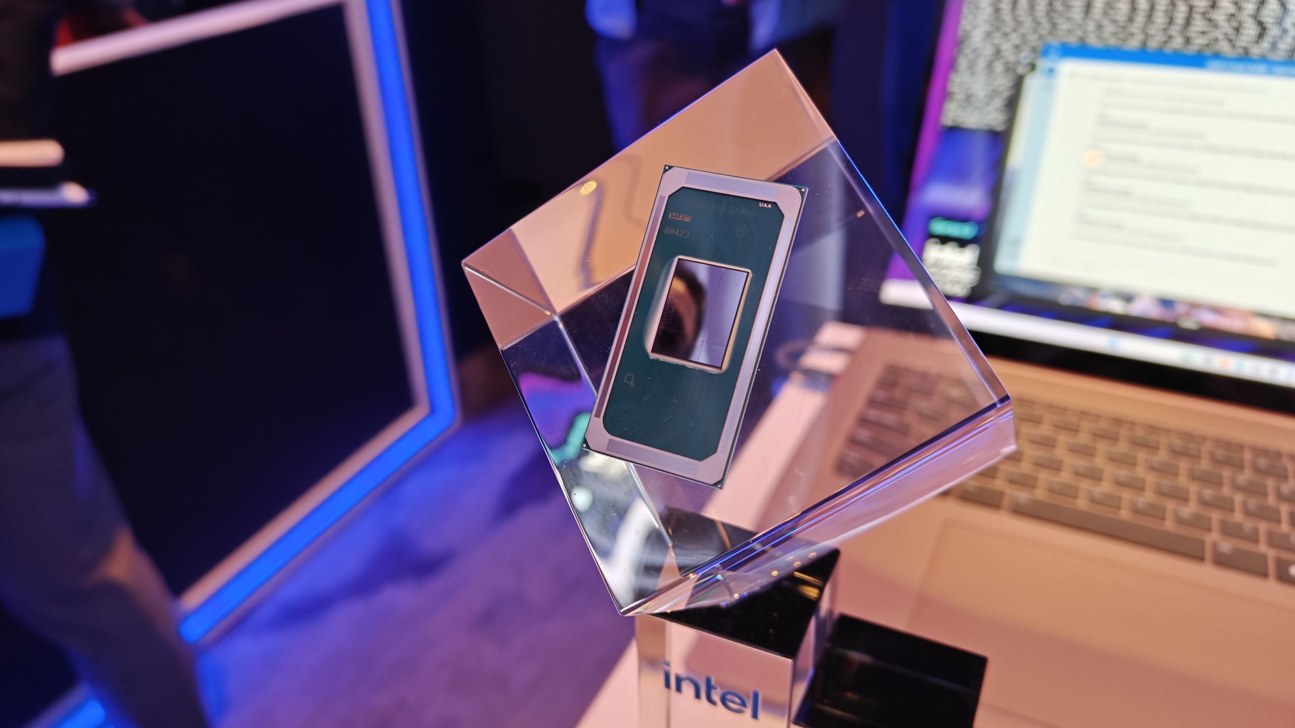
From 18A to 18A-P: A Rapid Evolution
The 18A node itself is foundational, introducing two revolutionary technologies: RibbonFET, Intel’s implementation of the Gate-All-Around (GAA) transistor architecture, and PowerVia, its pioneering backside power delivery system. RibbonFET offers superior gate control over traditional FinFET designs, leading to reduced leakage and improved switching speeds. PowerVia, on the other hand, reroutes power delivery to the backside of the wafer, freeing up the congested frontside for signal routing and significantly enhancing power integrity and thermal characteristics.
The development of 18A-P follows a well-established pattern of process optimization that chip manufacturers undertake to extract maximum value from a given node. After an initial "base" node is established, subsequent revisions often introduce minor tweaks, new IP blocks, or optimized device options to cater to specific performance, power, or density requirements. Intel had previously detailed aspects of 18A-P in a paper published earlier this year, setting the stage for the more comprehensive update provided at VLSI 2026. The motivation for 18A-P is clear: to continuously refine and push the boundaries of 18A, ensuring that Intel’s offerings remain competitive and adaptable to evolving market demands for high-performance and energy-efficient silicon. This iterative approach allows Intel to offer a more versatile and robust manufacturing platform to both internal product teams and external foundry customers.
The Significance of Risk Production
In the intricate world of semiconductor manufacturing, the journey from theoretical design to mass-produced silicon is meticulously structured. It typically begins with extensive research and development (R&D), followed by small-scale prototyping runs to validate fundamental concepts. "Risk production" is the critical bridge between these early experimental stages and full-scale high-volume manufacturing (HVM).
During risk production, the fabrication facility operates under conditions as close as possible to those of mass production. This involves utilizing the same production equipment, processes, and materials that will be employed for commercial products. However, the volume is deliberately kept low. The primary objectives are multi-faceted:
- Process Validation: To confirm that the entire manufacturing flow, from wafer preparation to final packaging, is stable and repeatable.
- Defect Rate Analysis: To identify and characterize any systematic defects or yield detractors that may emerge under production conditions. This data is crucial for process engineers to implement corrective actions.
- Performance Characterization: To ensure that the electrical characteristics (e.g., transistor speed, leakage, power consumption) of the fabricated chips meet design specifications consistently across the wafer and between different wafer lots.
- Variability Assessment: To understand the statistical variations in chip performance and characteristics, which is vital for binning products and ensuring quality control.
- Yield Improvement: While risk production itself is low-volume, the data gathered is instrumental in projecting and improving future yields for mass production.
For entirely new nodes, the period between risk production and HVM can span 12 to 24 months, allowing ample time for extensive testing, feedback loops, and process refinements. However, for an optimized revision like 18A-P, where the underlying 18A process is already ramping, this timeline is expected to be considerably tighter. This accelerated timeline suggests that Intel has a high degree of confidence in the foundational 18A technology and that 18A-P’s enhancements are more about refinement and expansion of capabilities rather than fundamental overhauls. The entry into risk production for 18A-P signals that Intel is rapidly approaching the commercial availability of chips leveraging these advanced capabilities.
Technical Deep Dive: Supporting Data and Architectural Enhancements
The improvements showcased with 18A-P are not merely incremental; they stem from sophisticated architectural and material science innovations. These advancements translate directly into more powerful and energy-efficient processors, impacting everything from consumer devices to massive data centers.
Performance and Efficiency Benchmarks
The headline figures of a 9% frequency increase or an 18% power reduction at 0.75 volts are significant. This 0.75V point is often considered a "sweet spot" for many modern processor workloads, representing a balance between performance and energy efficiency. By demonstrating improvements at this critical operating point, Intel is signaling that 18A-P-based chips will offer substantial gains in typical usage scenarios. For consumers, this could mean faster application loading, smoother multitasking, and longer battery life in laptops. For enterprise and data center clients, it translates to higher computational throughput per watt, enabling more work with less energy, which has profound implications for operational costs and environmental impact. Intel’s data also indicates that these frequency/power improvements are not limited to the 0.75V mark but are retained across a broader voltage range, demonstrating the robustness of the 18A-P optimization.
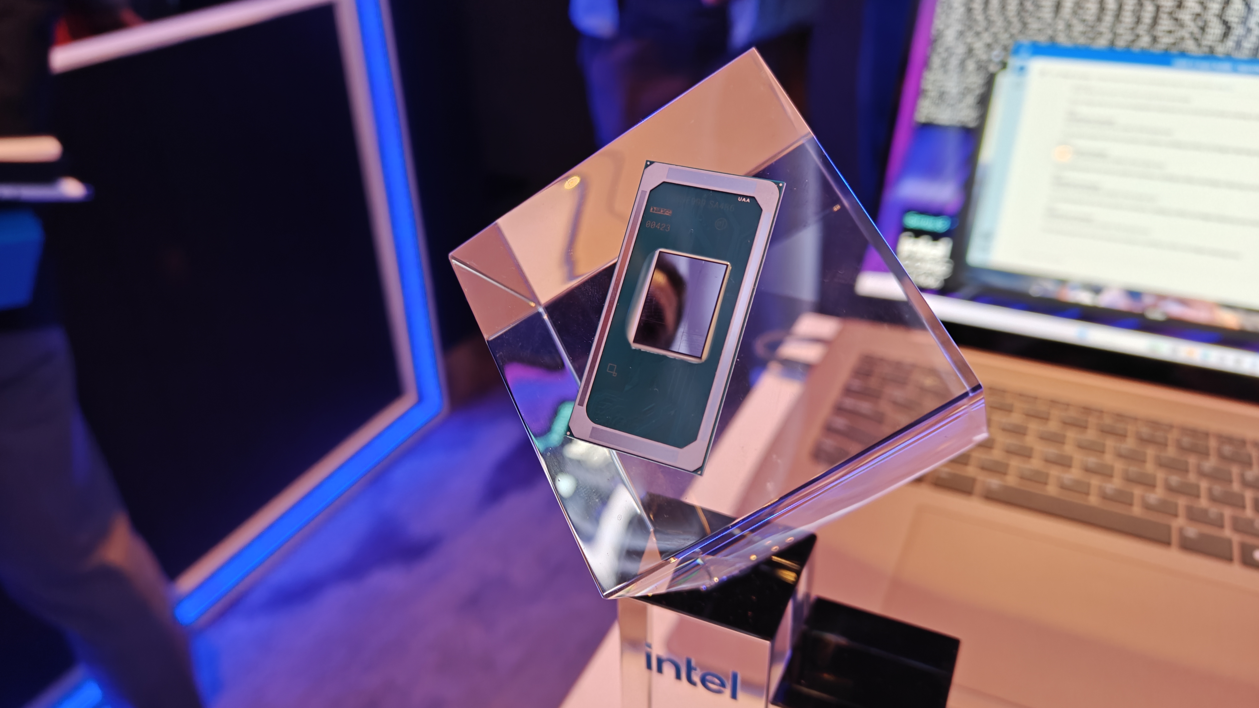
Transistor Innovations: Reshaping the Core
At the heart of 18A-P’s enhancements are crucial developments in transistor design, building upon the already advanced RibbonFET architecture. RibbonFET, Intel’s proprietary Gate-All-Around (GAA) transistor, is a fundamental shift from the FinFET architecture used in previous nodes. Unlike FinFETs, which have a gate wrapping around three sides of a fin-shaped channel, GAA transistors wrap the gate entirely around the channel (often in the form of multiple nanosheets or "ribbons"). This provides superior electrostatic control over the channel, significantly reducing leakage current and enabling faster switching speeds.
Complementing RibbonFET is PowerVia, Intel’s backside power delivery system. Traditionally, both power and signal lines are routed on the front side of the wafer, leading to congestion, increased parasitic resistance, and thermal challenges. PowerVia ingeniously routes power through the backside of the wafer. This innovation offers several key advantages:
- Reduced Congestion: Frees up the front side for denser and more efficient signal routing.
- Lower Interconnect Resistance: Shorter and wider power lines on the backside reduce resistance, improving power delivery efficiency.
- Enhanced Power Integrity: More stable voltage delivery to transistors.
- Improved Thermal Management: By separating power lines, it also contributes to better heat dissipation.
Building on these foundations, 18A-P introduces three new transistor designs to its library:
- W1 and W1.5: These are narrow designs optimized for low-power usage. The W1 design, previously available only in the 160mm cell height library, is now also accessible in the 180mm library. W1.5 is a new addition to the 160mm library. These additions fill critical gaps in Intel’s power-optimized design libraries, offering more granular control for designers aiming to create highly energy-efficient circuits.
- W3P (with "Power Boost"): This is perhaps the most intriguing new design. W3P is a new dual-contact transistor, meaning it establishes electrical contact on both the front side and the backside of the wafer. By leveraging the existing PowerVia backside connectivity, W3P significantly reduces parasitic resistance. This reduction in resistance enables a higher drive current, which directly translates to faster switching speeds for the transistor. The "Power Boost" capability of W3P is a direct consequence of this optimized power delivery, allowing for substantial frequency improvements in performance-critical paths. Even the original W2 and W3 designs, while not dual-contact, see a performance boost when implemented on the 18A-P process due to the overall process refinements and improved power delivery.
Enhanced Voltage Thresholds (VT) for Design Flexibility
Transistors operate based on a threshold voltage (VT), the minimum voltage required to turn them on. Different VT levels are crucial for chip designers to balance performance and power leakage. Typically, four flavors of VT pairs exist:
- HVT (High Threshold Voltage): Least performant, but lowest power leakage. Ideal for static, non-critical parts of a chip.
- SVT (Standard Threshold Voltage): A balance between performance and leakage.
- LVT (Low Threshold Voltage): More performant than SVT, but higher leakage. Used for moderately performance-sensitive areas.
- ULVT (Ultra-Low Threshold Voltage): Most performant, but highest power leakage. Reserved for critical, speed-demanding circuits.
With 18A-P, Intel is introducing a new VT pair: ULVTLL (Ultra-Low Voltage Threshold Low Leakage). This new option strategically positions itself between ULVT and LVT, offering better performance than LVT while exhibiting lower leakage than ULVT. This addition significantly enhances design flexibility, allowing engineers to fine-tune circuits more precisely for specific power-performance targets. For instance, designers can achieve higher clock speeds than with LVT without incurring the substantial power penalty associated with ULVT, making it ideal for sections of a chip that require high performance but also need to manage power consumption carefully, such as in mobile devices or certain AI accelerators.
Thermal and Interconnect Improvements
Beyond transistor and VT enhancements, 18A-P also brings crucial improvements to the physical integrity and thermal characteristics of the chip. Intel reports a 20% to 40% improvement in thermal resistance and a 10% to 30% improvement in via resistance at "perf critical layers."
- Thermal Resistance Reduction: Lower thermal resistance means heat can dissipate more effectively from the chip. This is achieved through advanced manufacturing techniques, including grinding the wafer down to optimize material properties for better thermal conductivity, and the use of sophisticated Electronic Design Automation (EDA) tools to simulate and optimize heat flow. For high-performance processors, reduced thermal resistance is paramount. It allows chips to sustain higher boost frequencies for longer periods, improves long-term reliability by reducing thermal stress, and potentially enables smaller, more efficient cooling solutions in end products.
- Via Resistance Improvement: Vias are vertical electrical connections that link different layers of a chip. "Perf critical layers" refer to the metal layers where high-speed signals are routed and where delays can significantly impact overall chip performance. Reducing via resistance in these critical areas directly translates to faster signal propagation and lower power loss. A 10% to 30% improvement is substantial, contributing to the overall frequency gains and power efficiency of the 18A-P process.
These detailed technical advancements collectively underscore Intel’s commitment to pushing the envelope in semiconductor manufacturing, laying the groundwork for a new generation of high-performance, power-efficient computing.
Industry Impact and Official Responses
The progress with 18A-P is not just a technical triumph; it carries significant strategic implications for Intel’s standing in the global semiconductor industry, particularly as it expands its foundry services.
Intel’s Foundry Services (IFS) Strategy
Under CEO Pat Gelsinger’s leadership, Intel has aggressively pursued a strategy to become a major player in the foundry market, manufacturing chips not only for its internal product divisions but also for external customers. This initiative, Intel Foundry Services (IFS), is crucial for diversifying Intel’s revenue streams and leveraging its vast manufacturing capabilities. The 18A node, and now its optimized variant 18A-P, are central to this strategy. Offering leading-edge nodes like 18A to external clients is vital for IFS to compete with established foundry giants like TSMC and Samsung. The superior performance and efficiency characteristics of 18A-P make it a highly attractive option for companies developing next-generation high-performance computing, AI, and mobile solutions. The reported talks with industry behemoths like Apple and Nvidia regarding potential future chip production on 18A highlight the growing interest and perceived competitiveness of Intel’s advanced nodes. Securing such high-profile clients would be a monumental validation of Intel’s foundry aspirations and its technological prowess.
Addressing Yield Challenges and Market Confidence
The journey to developing and mass-producing advanced semiconductor nodes is fraught with challenges, and Intel has not been immune to them. There have been reports and concerns regarding the initial yields of the 18A process, a common hurdle for any bleeding-edge manufacturing technology. Lower yields directly impact profitability and can deter potential customers.
However, Intel’s official response and the progression to 18A-P’s risk production paint a picture of improving conditions. The company has stated that defect rates for 18A continue to drop, and yields are improving in line with its internal expectations. This reassures the market that Intel is actively overcoming early manufacturing complexities. The decision to move 18A-P into risk production signifies a strong internal belief in the fundamental stability and scalability of the underlying 18A process. It suggests that the manufacturing kinks are being worked out, paving the way for consistent, high-volume production. Building market confidence is paramount for IFS, as external customers demand not only leading-edge technology but also reliable supply and predictable yields. Intel’s transparency and progress in addressing these challenges are crucial for establishing itself as a credible and competitive foundry partner.
Future Implications for the Semiconductor Landscape
The successful development and impending mass production of 18A-P carry far-reaching implications that could reshape the competitive dynamics of the semiconductor industry and fundamentally impact the capabilities of future computing devices.
Reshaping the Competitive Arena
Intel’s aggressive "five nodes in four years" strategy, culminating in 18A and its optimized variant 18A-P, is a direct challenge to the foundry dominance of TSMC and the competitive landscape with Samsung. If Intel can consistently deliver on its performance and yield targets for 18A-P, it could significantly alter the foundry services market. A robust and competitive Intel Foundry Services would provide a much-needed alternative source for advanced chip manufacturing, reducing reliance on a single primary vendor and potentially fostering greater innovation through competition.
For Intel’s traditional CPU rival, AMD, advancements in Intel’s process technology will inevitably influence future product strategies. While AMD currently relies on TSMC for its leading-edge manufacturing, a resurgent Intel with competitive or even superior process nodes could intensify competition in both the client (PC) and data center (server) segments. This could spur further innovation from all players, ultimately benefiting consumers and businesses through more powerful and efficient computing solutions.
Consumer and Enterprise Benefits
The technical improvements offered by 18A-P will translate into tangible benefits across a wide spectrum of applications. For the consumer market, laptops and desktops powered by Panther Lake CPUs will likely offer:
- Enhanced Performance: Faster processing for demanding applications, gaming, and creative workloads.
- Extended Battery Life: The 18% power reduction at equivalent performance will directly lead to longer operational times for mobile devices.
- Improved Thermal Management: Cooler-running devices, allowing for sustained high performance without throttling, and potentially enabling thinner, lighter form factors.
In the enterprise and data center space, Xeon 6+ processors leveraging 18A-P will bring:
- Higher Computational Density: More cores and greater processing power in the same physical footprint, optimizing data center real estate.
- Reduced Total Cost of Ownership (TCO): Lower power consumption per workload means significant energy savings, reducing electricity bills and cooling costs.
- Accelerated AI and HPC: The architectural enhancements, particularly the performance boosts and improved power delivery, are critical for accelerating complex AI models and high-performance computing tasks.
These advancements will drive the next wave of innovation in cloud computing, artificial intelligence, scientific research, and more, enabling capabilities that are currently challenging or impossible.
The Road Ahead: Sustaining Innovation
Intel’s journey with 18A and 18A-P is a testament to the iterative nature of semiconductor development, where continuous optimization is key to maintaining a competitive edge. The introduction of specific transistor designs like W3P and the new ULVTLL threshold voltage option highlights Intel’s commitment to providing chip designers with maximum flexibility and tools to create highly optimized silicon for diverse applications.
Looking ahead, the success of 18A-P will be crucial for Intel’s long-term vision. Beyond process nodes, Intel is also heavily investing in advanced packaging technologies like Foveros and EMIB, which allow for the integration of multiple chiplets onto a single package. The combination of leading-edge process nodes like 18A-P with sophisticated packaging solutions will be critical for achieving future performance and efficiency goals, enabling the creation of heterogeneous computing architectures tailored for specific workloads. As Intel moves closer to high-volume production of 18A-P, the industry will be watching closely to see how these innovations translate into real-world products and reshape the future of computing.

