TEXAS — In a move that could fundamentally reshape the global semiconductor supply chain, tech billionaire Elon Musk announced that critical manufacturing equipment suppliers, most notably lithography giant ASML, have expedited shipments for the unprecedented "Terafab" manufacturing complex. The revelation came during a live-streamed SpaceX Q3 earnings call on X, where Musk outlined aggressive timelines and massive capital commitments for the joint Tesla-SpaceX venture.
With an initial capital investment pegged at $16.8 billion and a projected footprint spanning an astonishing 100 million square feet of manufacturing space, the Terafab project represents one of the largest and most audacious industrial undertakings in modern history. Designed to fuel the future of autonomous vehicles, robotics, artificial intelligence, and aerospace infrastructure, the Texas-based project is moving at breakneck speed—though industry veterans warn that the timeline remains fraught with engineering hurdles.
Main Facts: The Scope of the Terafab Megaproject
The Terafab is not just another semiconductor fabrication plant (fab); it is an industrial behemoth designed to vertically integrate chip production on a scale never before attempted by a private conglomerate.
- The Visionaries: A joint strategic initiative between electric vehicle leader Tesla and aerospace pioneer SpaceX.
- Location: Gibbons Creek, Texas, a sprawling site chosen for its vast land availability and proximity to existing Texas tech and energy corridors.
- Scale: A staggering 100 million square feet of dedicated manufacturing and assembly space.
- Financial Commitment: An initial capital expenditure of $16.8 billion, though total outlays are widely expected to scale significantly as construction phases progress.
- Target Production Window: Volume chip production is aggressively slated for the third or fourth quarter of 2028.
- Key Suppliers: Accelerated supply chain commitments secured from industry titans, including ASML, the world’s premier provider of extreme ultraviolet (EUV) lithography systems.
Despite the grand scale of the announcement, Musk tempered expectations during the broadcast, explicitly noting that the 2028 production goal is "highly aspirational" and carries "big error bars," acknowledging the notoriously complex and bottleneck-prone nature of semiconductor fab construction.
Chronology: How the Terafab Concept Became Reality
The path from conceptual blueprint to accelerated equipment deliveries has been remarkably swift, defying the typical decades-long planning cycles associated with semiconductor manufacturing infrastructure.
The Genesis of Vertical Integration (2023–2024)
As global supply chains faced persistent shocks and geopolitical tensions threatened access to advanced nodes, both Tesla and SpaceX faced growing constraints in sourcing specialized silicon for their AI training clusters (such as Tesla’s Dojo), Full Self-Driving (FSD) hardware, and aerospace avionics. Musk began floating the concept of internalizing supply chains, moving away from pure reliance on third-party foundries like TSMC and Samsung.
Site Selection and Initial Land Acquisition (2025)
Rumors circulated throughout the tech industry regarding a massive industrial land grab in Texas. By mid-2025, plans coalesced around Gibbons Creek. The sheer acreage required—aiming for 100 million square feet—meant the facility would function less like a traditional cleanroom complex and more like a self-contained manufacturing city.
Formalizing the Tesla-SpaceX Alliance (Early 2026)
Rather than keeping the project siloed within a single corporate entity, Musk structured the Terafab as a collaborative megaproject between Tesla and SpaceX. This dual-company backing pooled engineering talent, capital reserves, and massive projected internal demand, making the project bankable on an unprecedented scale.
Supply Chain Lock-In and ASML Breakthrough (Late 2026)
The turning point arrived in October 2026. Securing advanced semiconductor equipment—particularly EUV and deep ultraviolet (DUV) lithography tools from ASML—typically requires a multi-year waiting list. However, during the Q3 2026 earnings call on October 20, Musk confirmed that ASML and other vital equipment vendors had agreed to expedite shipments, ensuring that critical hardware would arrive ahead of schedule to match the facility’s construction milestones.
Supporting Data: Breaking Down the Numbers
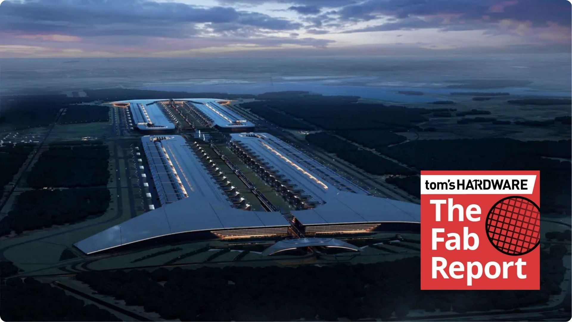
To understand the magnitude of the Terafab, it is helpful to place its metrics side-by-side with traditional semiconductor foundries.
| Metric | Traditional Mega-Fab (e.g., TSMC/Intel) | The Terafab Project |
|---|---|---|
| Total Footprint | 2 to 10 million square feet | ~100 million square feet |
| Initial Capital Investment | $10 billion – $20 billion (single phase) | $16.8 billion (initial phase) |
| Primary Beneficiaries | Broad market (Consumer, Mobile, PC, Automotive) | Internal ecosystem (Tesla AI, Robotics, SpaceX Avionics) |
| Primary Location Hubs | Taiwan, Arizona, Ireland, Germany | Gibbons Creek, Texas, USA |
| Target Operational Date | 3 to 5 years from breaking ground | Targeted Q3/Q4 2028 |
The sheer volume of the Terafab’s proposed footprint allows for co-located supply chains. Rather than shipping raw wafers, packaging components, and sub-assemblies across global logistics networks, the Terafab concept envisions housing raw material processing, wafer fabrication, advanced packaging (such as 3D chip stacking), and final product integration within a single geographic ecosystem.
Official Responses and Industry Reactions
The announcement has sent ripples through the global tech sector, eliciting a mix of awe, skepticism, and strategic maneuvering from competitors and policymakers alike.
The Supplier Perspective: ASML and Equipment Makers
While ASML has maintained a standard corporate policy regarding specific client negotiations, industry analysts note that securing expedited delivery slots implies unprecedented financial guarantees or prioritization agreements. ASML’s EUV systems are the lifeblood of sub-7nm chip manufacturing; without them, advanced AI and autonomous computing chips are impossible to produce at scale. The willingness of suppliers to bump the Terafab up their queue highlights the immense economic gravity Musk’s ventures now command.
Competitor and Foundry Fallout
Established foundries like Taiwan Semiconductor Manufacturing Company (TSMC), Samsung Electronics, and Intel are watching the Gibbons Creek development closely. While these giants possess decades of institutional know-how, process yields, and intellectual property that cannot be easily replicated, the entry of a massive, guaranteed-demand buyer building its own dedicated capacity changes the long-term semiconductor landscape. If successful, Tesla and SpaceX will effectively remove themselves as high-volume customers for external foundries, freeing up global capacity while simultaneously creating a formidable new domestic competitor.
Regulatory and Government Reception
Federal and state officials in Texas have largely welcomed the initiative. Coming on the heels of the federal CHIPS and Science Act, the Terafab aligns with broader national security goals aimed at reshoring advanced technology manufacturing onto American soil. State-level incentives and infrastructure support are widely expected to grease the wheels for the massive utility, water, and transportation networks required to sustain a 100-million-square-foot facility.
Implications: What the Terafab Means for the Future of Tech
The realization of a project of this scale carries profound implications for multiple industries, ranging from artificial intelligence to aerospace engineering.
1. Vertical Integration as the Ultimate Competitive Moat
For years, tech companies have relied on a fragmented supply chain—designing chips in-house, outsourcing fabrication to Asia, and assembling products globally. Musk’s strategy flips this script. By controlling the entire stack—from the silicon wafer rolling off the line in Texas to the neural net training on Tesla vehicles and the guidance computers on Starship rockets—Tesla and SpaceX minimize external vulnerabilities, slash logistics costs, and accelerate innovation cycles.
2. The Talent and Engineering Bottleneck
Despite the optimistic 2028 timeline and the successful securing of equipment shipments, industry experts emphasize that equipment is only half the battle. Operating a cutting-edge semiconductor fab requires an elite workforce of process engineers, materials scientists, and cleanroom technicians. Sourcing and training thousands of highly specialized personnel in rural or semi-rural Texas will arguably prove to be a more formidable obstacle than securing financing or hardware.
3. Redefining AI and Robotics Infrastructure
The primary driver behind the Terafab is the insatiable demand for compute power. As Tesla scales its humanoid robot program (Optimus), expands its Robotaxi fleet, and trains massive generative AI models, standard commercial chip supplies are projected to fall short. The Terafab guarantees a dedicated, uninterrupted supply of proprietary silicon optimized specifically for edge computing, neural network inference, and real-time robotics—potentially giving Tesla an insurmountable hardware advantage in the autonomous future.
Looking Ahead
As construction earthmovers prepare the Gibbons Creek site and expedited ASML shipping crates loom on the horizon, all eyes are fixed on Elon Musk’s 2028 deadline. While the timeline is universally acknowledged as aggressively optimistic, the combination of massive capital, supplier cooperation, and sheer industrial willpower ensures that the Terafab will be one of the most closely watched engineering endeavors of the decade.

