

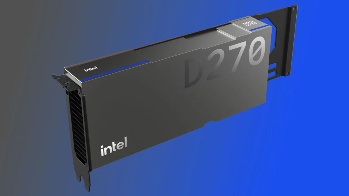
SAN JOSE, Calif. — At the Open Compute Project (OCP) Global Summit 2026, Intel Corporation finally lifted the veil on one of its most anticipated upcoming hardware architectures, shedding its internal codename in favor of a formal product identity. The silicon previously known throughout the industry as "Crescent Island" has been officially christened the Intel GPU D-Series.
Alongside the official product naming, Intel used the OCP 2026 stage to deliver a cascade of crucial performance metrics. For the first time, the semiconductor giant publicly outlined the theoretical peak performance capabilities of the chip, targeting a formidable 1.3 PFLOPS (petaflops) of FP8 compute. Furthermore, the company clarified the memory subsystem specifications, confirming a final memory bandwidth of 1.5 TB/s paired with an astonishing capacity of up to 480GB of LPDDR5X memory.
This comprehensive disclosure marks a major inflection point in Intel’s protracted strategy of dropping incremental hints about Crescent Island throughout 2026. As the artificial intelligence landscape shifts increasingly toward the economic and operational realities of scalable inference, Intel’s newly minted GPU D-Series positions itself as a specialized, high-density workhorse engineered specifically to shoulder the massive computational burdens of modern large language models (LLMs) and deep learning workloads.
Main Facts
The announcement at OCP 2026 solidifies the core technical parameters of the Intel GPU D-Series, transforming speculative industry gossip into verified architectural specifications. At its foundation, the D-Series is not a traditional graphics processor in the consumer sense. Instead, it is a dedicated massively parallel computing accelerator built from the ground up for high-efficiency data center workloads.
Key takeaways from the OCP 2026 disclosures include:
- Official Branding: The codename "Crescent Island" has been officially retired in favor of the Intel GPU D-Series.
- Compute Performance: The chip boasts a theoretical peak performance target of 1.3 PFLOPS of FP8 (8-bit floating-point) computational throughput.
- Memory Subsystem: The accelerators will feature a robust final memory bandwidth of 1.5 TB/s, coupled with an unprecedented up to 480GB of LPDDR5X memory on board.
- Architecture: The GPU D-Series represents the commercial debut of Intel’s advanced Xe3P graphics and parallel computing architecture.
- Form Factor and Power: Products within the D-Series lineup will be delivered in an air-cooled PCIe form factor with a Thermal Design Power (TDP) cap of 350W.
Unlike traditional GPUs laden with display controllers, texture mapping units, and hardware ray-tracing pipelines, the Xe3P architecture strips away graphics-specific functional units to maximize silicon area for raw, parallel data processing. This specialization is tailored to maximize performance-per-watt metrics for data centers grappling with power and cooling constraints.
Chronology of Disclosures: The Road to OCP 2026
The journey toward the official unveiling of the Intel GPU D-Series has been characterized by a calculated, methodical release of information. Intel has utilized a "slow drip" disclosure strategy across various industry events and investor briefings throughout 2026, building anticipation while keeping competitors guessing about the true scope of their next-generation accelerator.
Early 2026: The Whispers of "Crescent Island"
Rumors surrounding Crescent Island first began circulating within high-performance computing (HPC) circles in the opening weeks of 2026. Industry analysts noted references in software toolchains and compiler updates pointing to a mysterious, highly specialized compute engine being developed under the codename. Early leaks suggested that Intel was designing a non-graphics parallel processor meant to bypass traditional high-bandwidth memory (HBM) supply chain bottlenecks by leveraging alternative memory technologies.
Spring 2026: Confirming the Xe3P Foundation
By mid-spring, Intel executives began acknowledging the existence of the chip during private briefings and select technical conferences. It was during this period that the company confirmed Crescent Island would serve as the vanguard for the Xe3P architecture. Engineers clarified the "P" designation, explaining that the architecture was engineered from the ground up for massively parallel workloads, intentionally shedding legacy graphics pipelines to optimize die space and power efficiency.
Summer 2026: Teasing Form Factors and Power Envelopes
As summer progressed, secondary details regarding the physical implementation of the chip trickled out. Industry insiders learned that Intel was prioritizing air-cooled server infrastructures rather than immediately demanding liquid-cooling loops—a crucial consideration for enterprise data centers seeking to upgrade legacy server racks without undertaking expensive infrastructure overhauls. Rumors regarding a 350W power envelope and massive LPDDR5X footprints began gaining traction among hardware sleuths.
Fall 2026 (OCP Global Summit): The Grand Unveiling
The culmination of this information campaign arrived at the OCP Global Summit 2026. By officially naming the product the Intel GPU D-Series and dropping exact figures for FP8 performance (1.3 PFLOPS) and memory bandwidth (1.5 TB/s), Intel moved the architecture out of the speculative phase and firmly into the commercialization pipeline.
Supporting Data and Architectural Analysis
To truly understand where the Intel GPU D-Series fits into the modern data center ecosystem, one must examine the intersection of its compute density, memory architecture, and power delivery mechanisms.
Breaking Down the Numbers: 1.3 PFLOPS of FP8
The modern AI era is defined by quantization. While training massive foundation models often requires FP16 or BF16 precision, inference—the process of running a trained model to generate responses or classifications—thrives on lower-precision formats like FP8. By targeting 1.3 PFLOPS of FP8 performance, Intel is squarely targeting the high-throughput inference market.
To put this in perspective, delivering over a petaflop of low-precision compute within a standard accelerator footprint allows hyperscalers to deploy dense clusters capable of processing millions of token requests per second. However, raw compute is only half the battle; feeding data to those execution units fast enough is the true architectural bottleneck.
The LPDDR5X Advantage: 480GB and 1.5 TB/s
Perhaps the most intriguing aspect of the GPU D-Series hardware specification is its reliance on LPDDR5X memory rather than traditional High Bandwidth Memory (HBM3e or HBM4).
- Massive Capacity: By packing up to 480GB of LPDDR5X memory onto the accelerator, Intel is directly addressing the memory capacity bottleneck that plagues large language model inference. Loading massive LLMs requires immense VRAM space. While HBM offers staggering bandwidth, its capacity per stack has historically lagged behind what system integrators desire for holding gargantuan model weights locally on a single card.
- Bandwidth Mechanics: Delivering 1.5 TB/s of memory bandwidth via LPDDR5X is a remarkable engineering feat, achieved through wide memory buses and high-frequency operation. While 1.5 TB/s is lower than top-tier HBM solutions, the trade-off yields a dramatically higher memory capacity-to-cost ratio and avoids the notoriously supply-constrained HBM manufacturing ecosystem.
Thermal and Power Efficiency: The 350W Sweet Spot
Modern data centers are running into severe power and cooling walls. Many legacy server racks are rated for maximum thermal envelopes of 350W to 500W per slot, making liquid cooling mandatory for extreme-wattage accelerators (which frequently exceed 700W to 1000W).
By anchoring the GPU D-Series at a 350W TDP in an air-cooled PCIe form factor, Intel has deliberately designed the card for drop-in compatibility. Enterprises can slide the D-Series into existing standard server chassis without needing to retrofit data center cooling systems, drastically lowering the total cost of ownership (TCO) for deployment.
Official Responses and Industry Perspectives
Intel’s executive leadership and technical fellows have framed the OCP 2026 announcements as a validation of the company’s pivot toward practical, scalable AI infrastructure.
During his keynote address at OCP 2026, Intel’s senior vice president of accelerated computing emphasized that the industry’s obsession with raw, unconstrained power scaling is hitting a wall. "The future of AI is not just about building the most expensive, power-hungry monolithic chip possible," the executive noted. "It is about democratizing inference through architectural efficiency. With the GPU D-Series and the Xe3P architecture, we are delivering the exact balance of massive low-precision compute and unprecedented memory capacity that cloud service providers need to make large-scale AI economically viable."
Early reactions from industry analysts and OCP attendees have been cautiously optimistic. Hardware analysts pointed out that while NVIDIA and AMD currently dominate the high-end training and inference conversation with their respective HBM-based accelerators, Intel’s unique approach—trading peak HBM bandwidth for massive LPDDR5X capacity—carries a distinct economic advantage.
"If Intel can deliver 480GB of LPDDR5X at a disruptive price point, they carve out a very lucrative niche," noted an enterprise infrastructure analyst present at the summit. "There are countless enterprise customers who cannot afford or cool massive liquid-cooled clusters, yet they desperately need high-capacity VRAM to host local, private LLMs. The GPU D-Series looks tailor-made for that exact demographic."
Software developers within the OCP community also welcomed the formalization of the Xe3P architecture details. Predictable access to hardware targets allows compiler teams and framework maintainers (such as those working on PyTorch and Triton optimizations) to tune their backends ahead of hardware availability, ensuring a smoother software rollout when production units begin shipping.
Implications for the AI Hardware Market
The formal unveiling of the Intel GPU D-Series carries profound implications for the broader semiconductor landscape, the cloud infrastructure market, and the economics of artificial intelligence deployment.
1. Disrupting the HBM Monopoly
For the past several years, High Bandwidth Memory has been the ultimate chokepoint in the AI hardware supply chain. Driven by intense demand from the booming generative AI sector, HBM packaging capacity has routinely fallen short of market demand, keeping accelerator prices artificially high. By demonstrating that high-capacity LPDDR5X can be successfully leveraged to build a high-performance inference accelerator (1.5 TB/s bandwidth with up to 480GB capacity), Intel is proving that alternative memory topologies are viable at the enterprise level. If successful, this could pressure memory manufacturers to diversify architectures and lower costs across the board.
2. A Shift in Focus from Training to Inference Economics
As foundation models mature, the industry cost structure is undergoing a seismic shift. While model training remains an elite, compute-heavy endeavor dominated by a handful of massive tech titans, inference is becoming a ubiquitous utility required by every enterprise software company on the planet. Inference economics are governed entirely by cost-per-token, power consumption, and hardware acquisition costs. The Intel GPU D-Series—with its air-cooled 350W envelope, standard PCIe form factor, and massive local memory pool—is fundamentally an inference-first machine. Its market success could signal a broader industry trend away from monolithic, hyper-expensive training monsters toward modular, cost-effective inference workhorses.
3. Intel’s Foundry and Product Strategy Redemption
For Intel, executing successfully on the Xe3P architecture and the D-Series product line is a critical test of credibility. Following a turbulent few years marked by strategic realignments and fierce competition on multiple fronts, proving that its advanced parallel computing architectures can deliver competitive metrics in the data center is vital. If the GPU D-Series can capture meaningful market share in enterprise inference deployments, it will validate Intel’s multi-generation architectural roadmap and reassure investors of the company’s long-term viability in high-performance silicon.
Outlook and Next Steps
As the OCP Global Summit 2026 draws to a close, attention now turns to the software ecosystem and the eventual hardware validation phase. While Intel has provided the theoretical peak performance targets (1.3 PFLOPS FP8) and architectural boundaries (Xe3P, 1.5 TB/s, up to 480GB LPDDR5X, 350W TDP, PCIe air-cooled), independent benchmark validation will ultimately dictate the market reception of the GPU D-Series.
Enterprise customers and cloud service providers will be watching closely for early engineering samples and software stack maturity reports in the coming quarters. If Intel can couple these impressive hardware specifications with a robust, reliable, and developer-friendly software ecosystem—leveraging its open-source initiatives and deep framework integrations—the Intel GPU D-Series may well transform from a codename on a roadmap into a foundational pillar of the next generation of enterprise artificial intelligence infrastructure.

