

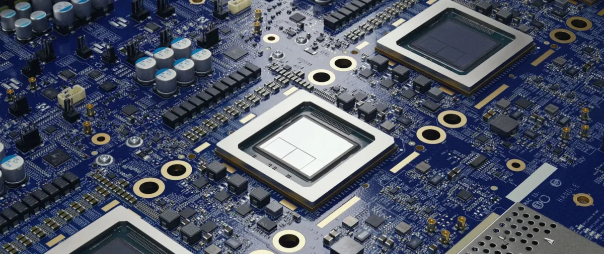
SAN FRANCISCO — In the relentless pursuit of computational supremacy, the semiconductor industry has reached a historic, albeit dizzying, inflection point. In late August, tech startup Architect Labs made headlines across the technology sector by claiming it had successfully designed a microprocessor almost entirely developed by artificial intelligence—a feat widely hailed as an industry first.
While AI has quietly embedded itself into the multi-billion-dollar semiconductor manufacturing workflow over the past decade, Architect Labs’ milestone suggests a fundamental shift. We are no longer merely using artificial intelligence as a sophisticated calculator or a glorified spellchecker for code; we are entering an era where AI is actively authoring the physical substrate of its own future evolution.
This development accelerates a profound recursive feedback loop: modern AI models, running on hardware designed by human engineers with computational assistance, are now drafting the architectures for the next generation of silicon. That silicon, in turn, will power even more advanced AI models. As electronic design automation (EDA) vendors and semiconductor giants cede larger swaths of the drafting table to autonomous agents, the boundary between creator and creation is beginning to blur.
Main Facts
The modern semiconductor design workflow is notoriously complex, prohibitively expensive, and constrained by a severe global shortage of specialized engineering talent. Designing a cutting-edge processor requires navigating billions of microscopic transistors, managing extreme thermal dissipation, minimizing signal delay, and optimizing power consumption—all within microscopic margins of error.
To cope with this staggering complexity, the industry has spent years integrating machine learning into specific phases of the pipeline. Traditionally, AI’s role was auxiliary. Algorithms were deployed to handle tedious, computationally brute-force tasks such as:
- Floorplanning: Determining the optimal physical placement of major functional blocks on a silicon die.
- Placement and Routing (P&R): Mapping out the intricate microscopic wiring that connects billions of transistors.
- Verification and Simulation: Running millions of test vectors to catch logic bugs before tape-out.
However, the leap demonstrated by Architect Labs and supported by broader industry trends involves Generative AI and Agentic Systems. Unlike static algorithms that optimize a pre-defined layout, modern generative tools can assist engineers in writing and refining Register-Transfer Level (RTL) code—the blueprint that describes hardware behavior.
Concurrently, emerging agentic workflows can operate Electronic Design Automation (EDA) software autonomously. These systems can execute simulations, analyze performance metrics, pinpoint design bottlenecks, modify the underlying code to resolve issues, and iterate on the process continuously with drastically reduced human intervention.
Despite these autonomous leaps, a critical boundary remains: human engineers still define the overarching high-level architectures, establish core performance targets, and make the foundational trade-offs regarding what a chip is meant to achieve. But as agentic systems grow more robust, that human-dominated perimeter is steadily shrinking.
Chronology of AI Integration in Chip Design
To understand the magnitude of Architect Labs’ recent milestone, it is essential to trace how artificial intelligence steadily infiltrated the conservative, high-stakes world of semiconductor engineering over the past decade.
Phase 1: Statistical Optimization and Machine Learning Assistants (2016–2019)
Long before generative models captured the public imagination, major EDA companies like Synopsys and Cadence, alongside academic researchers, began deploying classical machine learning algorithms to solve NP-hard optimization problems in physical layout design. Floorplanning, in particular, became an early proving ground. While human engineers still drew the blueprints, ML models could sort through trillions of possible floorplans in days rather than months, often beating human experts at raw wire-length minimization.
Phase 2: The Google TPU Breakthrough (2020–2021)
A watershed moment occurred when Google published research detailing how its reinforcement learning agents could design the floorplanning for its Tensor Processing Unit (TPU) chips in a fraction of the time required by human teams. Google’s approach treated chip floorplanning like a game of Go or chess, rewarding the AI for minimizing power, performance, and area (PPA) metrics. While controversial within certain academic circles regarding its baseline comparisons, the industry took notice: reinforcement learning could yield production-ready silicon layouts.
Phase 3: The Generative AI Boom and RTL Acceleration (2022–2023)
Following the explosive commercialization of Large Language Models (LLMs), the semiconductor industry rushed to adapt transformer architectures to hardware description languages (HDLs) like Verilog and VHDL. AI models proved remarkably capable of translating natural language prompts into working RTL code snippets, accelerating the most tedious phases of logic design and helping junior engineers navigate legacy codebases.
Phase 4: Agentic EDA and Full-Cycle Autonomy (2024–Present)
The current era is defined by the shift from static code-completion tools to dynamic agentic systems. Companies are no longer just using AI to write a single function; they are deploying multi-agent frameworks capable of closing the loop between writing RTL, running EDA verification software, reading error logs, and rewriting code autonomously. Architect Labs’ August disclosure represents the vanguard of this phase—a system capable of driving the design process from high-level parameters close to a complete, manufacturable database with minimal human intervention.
Supporting Data and Technical Realities
The transition toward AI-driven chip design is not merely driven by a desire for novelty; it is an economic and physical imperative. Moore’s Law—the observation that the number of transistors on a microchip doubles roughly every two years—has slowed down considerably, while the cost of designing a leading-edge 3nm or 2nm chip has skyrocketed past the half-billion-dollar mark.
| Development Stage | Traditional Human-Led Approach | AI-Assisted / Agentic Approach |
|---|---|---|
| Architectural Definition | 100% Human driven; years of exploratory research. | Primarily human-driven, with AI generating scenario models. |
| RTL Code Generation | Manual coding, prone to syntax and logic oversights. | LLM-accelerated generation; rapid prototyping of modules. |
| Floorplanning & P&R | Months of manual tweaking; heuristic-based EDA tools. | Reinforcement learning exploring trillions of layouts simultaneously. |
| Verification & Bug Hunting | Slow, manual testbench creation; massive compute clusters. | Autonomous agent loops executing continuous regression testing. |
According to recent analyses from academic researchers at institutions like UC Berkeley, while LLMs and agentic tools are beginning to out-design human engineers in narrow, highly constrained sub-domains (such as optimizing specific arithmetic logic units or power-gating networks), they remain dependent on human guidance for systemic context.
Furthermore, the data reveals a widening gap in productivity. Semiconductor firms leveraging machine learning optimization in their EDA flows report layout cycle-time reductions of up to 50%, allowing smaller engineering teams to tackle projects that previously required hundreds of specialized layout designers. However, this efficiency introduces new bottlenecks: verifying that an AI-generated chip is entirely free of subtle, catastrophic logic flaws requires immense computational verification infrastructure, as human engineers must audit code they did not personally author.
Official Responses and Industry Perspectives
The announcement by Architect Labs and the broader trend of autonomous EDA tools have triggered a spectrum of reactions across the tech industry, ranging from unbridled optimism to cautious skepticism.
Dr. Evelyn Vance, Chief Technology Officer at a major EDA software provider, noted during a recent industry panel:
"We are moving past the era where AI is just a feature inside a software suite. AI is becoming the primary interface between human intent and silicon reality. The question is no longer whether AI can design chips, but how quickly we can build verification safeguards robust enough to trust what the agents create."
Conversely, veteran silicon architects have sounded notes of caution regarding the "black box" nature of AI-generated hardware. Because neural networks arrive at solutions through statistical optimization rather than deductive reasoning, understanding why an AI chose a specific routing path or transistor sizing can be exceptionally difficult.
Marcus Thorne, a senior hardware fellow with over thirty years of experience designing CPUs, remarked:
"An AI can optimize PPA metrics brilliantly, but it doesn’t possess engineering intuition. If an edge-case environmental stressor occurs in the field—say, a voltage spike combined with extreme thermal throttling—an AI-designed layout might fail in ways a human architect would have anticipated because we understand the physical physics of the silicon on a fundamental level. We cannot afford black-box surprises in mission-critical or automotive silicon."
Meanwhile, venture capitalists and startup founders are betting heavily on the democratization of chip design. By lowering the financial and human capital barriers to custom silicon, AI tools are expected to fuel a renaissance of domain-specific accelerators—custom chips tailored precisely for specific workloads like quantum simulation, genomics, and localized edge-AI inference.
Broader Implications
The advent of AI-designed hardware carries profound geopolitical, economic, and technological implications that extend far beyond Silicon Valley.
1. The Democratization of Custom Silicon
Historically, designing a custom ASIC (Application-Specific Integrated Circuit) was an exclusive luxury reserved for tech titans like Apple, Google, Nvidia, and Qualcomm, who could afford hundreds of millions of dollars in engineering salaries and tool licenses. As agentic EDA systems automate the grueling mechanics of layout and verification, smaller enterprises and academic labs may soon design proprietary silicon tailored to their specific software stacks, upending the traditional merchant semiconductor market.
2. The Acceleration of the AI Singularity Loop
Perhaps the most profound implication is the recursive nature of the technology. For years, the bottleneck in artificial intelligence development has been hardware: training massive frontier models requires thousands of specialized GPUs and TPUs. If AI can design faster, more power-efficient, and cheaper processors for machine learning, the cost-per-flop of computation will plummet. This creates a hyper-accelerated feedback loop where better software builds better hardware, which in turn builds vastly superior software.
3. Shifts in the Semiconductor Workforce
The role of the hardware engineer is undergoing a tectonic shift. The tedious, repetitive aspects of logic entry, netlist debugging, and physical layout optimization are rapidly being automated away. Consequently, the industry demands a different kind of talent: engineers who excel at systems-level thinking, prompt engineering for hardware, safety verification, and architectural oversight. The future silicon architect will resemble an orchestral conductor, guiding and auditing fleets of autonomous software agents rather than manually drawing polygons on a screen.
Conclusion
Architect Labs’ breakthrough in late August is likely just the opening salvo in a broader transformation of the semiconductor industry. As artificial intelligence transitions from an assistant in the design room to a primary architect of silicon, the boundaries of what is possible in computing are expanding at an unprecedented rate.
We are stepping across a historic threshold: humans are training intelligence systems, those systems are writing the code for the hardware of tomorrow, and that very hardware will wake up to power the next generation of artificial minds. In this new paradigm, the silicon ceiling is no longer defined by human imagination or manual labor, but by the velocity of our recursive technological evolution.

