

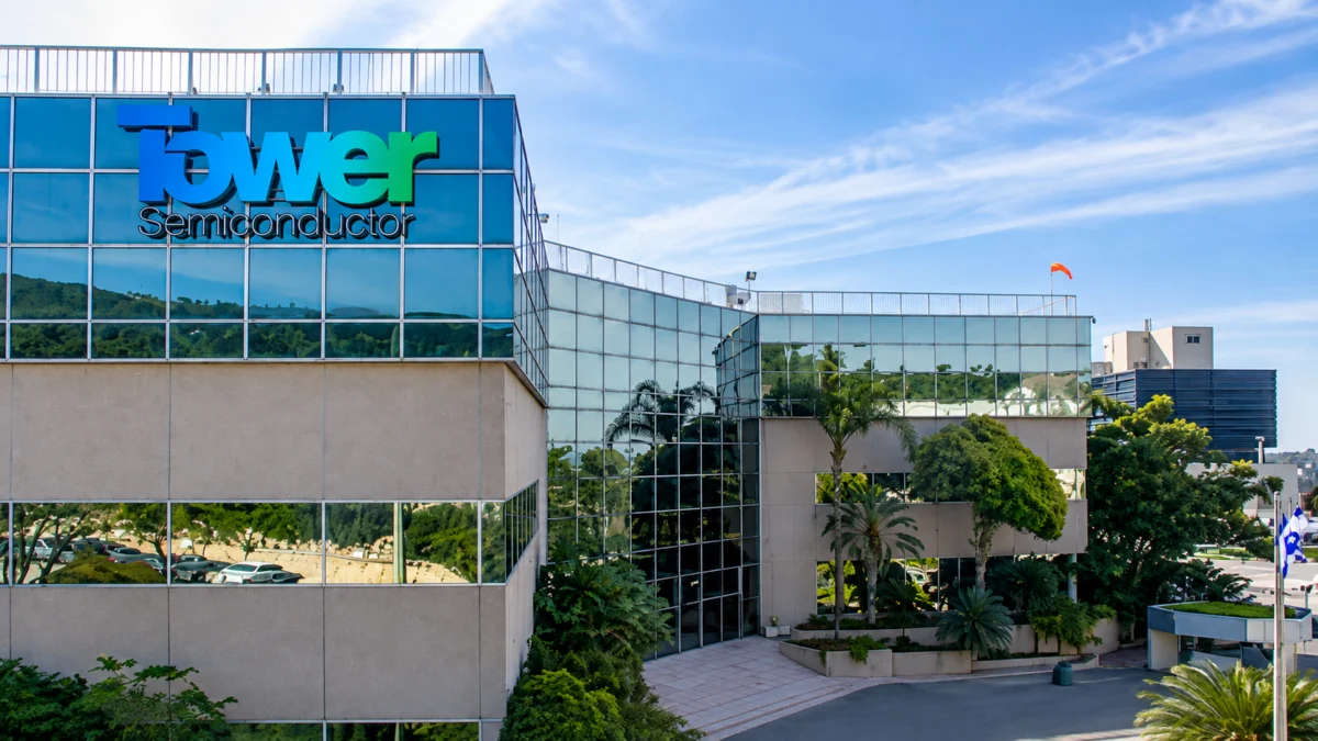
TOKYO / MIGDAL HAEMEK — In a landmark move poised to reshape the global semiconductor landscape, specialty foundry leader Tower Semiconductor has announced a massive $4 billion joint investment with the Japanese government. The ambitious initiative aims to restructure and dramatically expand Tower’s regional footprint, turning Japan into the company’s primary manufacturing base for next-generation optical-connectivity semiconductors.
The multi-year, dual-track expansion strategy is designed to catapult Tower’s local production capabilities to unprecedented heights, targeting a staggering 40-fold increase in output by 2029. By capitalizing on soaring global demand for high-speed data transmission components—driven largely by the explosive growth of artificial intelligence (AI) data centers and cloud computing—this strategic pivot highlights Japan’s continuing resurgence as a powerhouse in the international chip-manufacturing ecosystem.
Main Facts
The core of the $4 billion project revolves around a comprehensive overhaul and expansion of Tower Semiconductor’s manufacturing infrastructure in Japan. According to reports from Nikkei, the joint funding initiative between the Israeli-headquartered foundry and Japanese authorities will unfold through a sophisticated, multi-phase strategy.
- Massive Financial Commitment: A combined investment of $4 billion is being funneled into Tower’s Japanese operational framework.
- Target Output: The dual-track expansion aims to radically increase production capacity to the equivalent of 45,000 300mm wafers per month by the year 2029. This represents a roughly 40-fold scaling of the company’s current output in the region.
- Strategic Focus: The facilities will specialize in advanced optical-connectivity semiconductors—critical hardware components that utilize light rather than electrical signals to move data at ultra-high speeds across vast networks.
- Infrastructure Strategy: The project involves repurposing an idle fabrication plant, optimizing an existing 300mm wafer fab, and ultimately constructing a brand-new 300mm manufacturing facility to meet projected long-term demand.
Chronology of the Expansion
The path toward establishing Japan as an optical semiconductor powerhouse has been carefully mapped out by Tower Semiconductor’s executive leadership in tandem with regional stakeholders. The timeline envisions a phased rollout that balances immediate capacity maximization with long-term infrastructure development.
Phase 1: Operational Restructuring and Initial Optimization (2023–2024)
Before committing to multi-billion-dollar outlays, Tower initiated a strategic reorganization of its Japanese business entities to streamline decision-making and operational efficiency. During this period, the company evaluated existing assets, identifying underutilized real estate and idle manufacturing space ripe for modernization. Concurrently, initial dialogues with the Japanese government laid the groundwork for public-private financial backing, aligning with Tokyo’s broader national strategy to secure domestic semiconductor supply chains.
Phase 2: Track One — Conversion and 300mm Maximization (2025–2026)
The immediate execution phase focuses heavily on Track One of the dual-track strategy. This involves taking an idled semiconductor fabrication facility and systematically converting it to handle modern manufacturing processes. At the same time, Tower will maximize the output of its existing 300mm wafer facility in the region. By modernizing legacy cleanrooms and installing state-of-the-art lithography and etching tools tailored for optical components, Tower expects to see early, substantial increments in wafer throughput.
Phase 3: Track Two — Greenfield Construction and Scaling (2027–2028)
As existing converted facilities approach peak utilization, the initiative transitions into Track Two. This phase centers on breaking ground and constructing an entirely new 300mm wafer fabrication plant. This greenfield project will be specifically designed from the ground up to accommodate the unique thermal, chemical, and precision requirements associated with optical-electronic integration and silicon photonics manufacturing.
Phase 4: Full Maturity and Target Capacity (2029)
By the close of the decade, the combined output of the repurposed fab, the optimized legacy 300mm plant, and the newly constructed facility is projected to hit the milestone target of 45,000 300mm equivalent wafers per month. At this juncture, Tower’s Japanese hub will be fully operational, functioning as a primary global nexus for high-speed optical connectivity chips.
Supporting Data and Market Dynamics
To understand the magnitude of Tower Semiconductor’s $4 billion bet, one must examine the macroeconomic and technical forces currently reshaping the semiconductor industry.
The Bottleneck of Modern Data Transfer
As generative AI models, large language models (LLMs), and hyper-scale cloud infrastructures scale to unprecedented sizes, traditional copper-based interconnects are hitting severe physical limits. Copper cables suffer from signal attenuation, high power consumption, and bandwidth throttling over long distances—challenges that become acute inside massive server clusters housing tens of thousands of AI accelerators (such as GPUs and custom ASICs).
Optical connectivity chips solve this dilemma by converting electrical data streams into optical signals using light pulses. This enables ultra-fast, low-latency, and energy-efficient data transmission between server racks and across data center networks. However, manufacturing these chips is notoriously complex, requiring specialized foundry processes that merge standard silicon technology with optical components (silicon photonics).
Capacity Scaling Metrics
To contextualize Tower’s goal of 45,000 300mm equivalent wafers per month by 2029:
- Current Output: Tower’s historical footprint in the region operated at a significantly smaller scale, making a 40-fold increase one of the most aggressive capacity scaling initiatives undertaken by a specialty foundry in recent years.
- Wafer Size Transition: Shifting operations predominantly to 300mm (12-inch) wafers—rather than older, smaller 200mm (8-inch) standards—allows for vastly superior economies of scale, drastically reducing the cost-per-chip for high-volume enterprise customers.
- Global Footprint Integration: While Tower maintains operations in Israel and the United States (through partnerships and its own facilities), the Japanese hub will effectively become the crown jewel of its optical-chip manufacturing portfolio.
Official Responses and Strategic Partnerships
The collaboration between Tower Semiconductor and the Japanese government is emblematic of a broader global trend where national governments actively subsidize and incentivize semiconductor manufacturing within their borders to insulate themselves from geopolitical and supply chain vulnerabilities.
Government Support and Economic Security
Japan’s Ministry of Economy, Trade and Industry (METI) has been aggressive in revitalizing the nation’s semiconductor sector. Over the past few years, Tokyo has poured tens of billions of dollars into attracting foreign foundries—including TSMC, Micron, and Powerchip—while simultaneously supporting domestic champions like Rapidus.
The partnership with Tower Semiconductor fits neatly into this grand strategy. While many international investments in Japan have focused heavily on legacy logic or advanced computing nodes, Tower’s specialization in analog, mixed-signal, and optical-connectivity chips fills a crucial niche. Japanese officials have emphasized that securing a dominant domestic supply of optical components is vital for maintaining the nation’s technological competitiveness in telecommunications, automotive systems, and AI infrastructure.
Tower Semiconductor Leadership Perspective
For Tower Semiconductor, the investment represents a transformative corporate milestone. Executives have noted that the partnership allows the company to rapidly scale without bearing the entirety of the capital expenditure burden on its balance sheet. By leveraging Japanese state backing, Tower can accelerate its roadmap, secure long-term purchase commitments from major global tech conglomerates, and solidify its position as the go-to specialty foundry for photonics and optical connectivity.
Industry analysts have praised the move as a masterclass in strategic positioning. By anchoring its optical operations in Japan—a country renowned for its precision engineering, skilled workforce, and robust supply chain infrastructure—Tower mitigates geographic risks while placing itself at the epicenter of the next great technological transition.
Implications for the Tech Industry
The successful execution of Tower Semiconductor’s $4 billion Japanese expansion project will carry profound implications across multiple sectors of the global technology landscape.
1. Easing the AI Infrastructure Bottleneck
The explosive demand for AI hardware has often overshadowed the supporting infrastructure required to keep data flowing seamlessly. Without advanced optical transceivers and silicon photonics, the fastest GPUs in the world are inevitably bottlenecked by communication delays between servers. Tower’s massive influx of optical chips into the global supply chain will help alleviate these bottlenecks, enabling the construction of even larger, more efficient AI data centers.
2. The Rise of Specialized Foundries
For decades, the semiconductor narrative was dominated by massive, general-purpose logic foundries producing smartphone and PC processors on cutting-edge nodes (e.g., 3nm and 2nm). However, the future increasingly belongs to heterogeneous integration and specialty technologies—such as analog, radio frequency (RF), power management, and photonics. Tower’s heavy investment validates the immense commercial viability of specialty foundries, proving that companies do not necessarily need to chase the smallest digital transistor nodes to command multi-billion-dollar markets.
3. Japan’s Semiconductor Renaissance
This initiative further cements Japan’s successful return as a dominant force in global chipmaking. Once a leading semiconductor manufacturer in the late 20th century before experiencing decades of decline, Japan has orchestrated a remarkable comeback through targeted financial subsidies, streamlined regulatory frameworks, and welcoming foreign partnerships. With Tower building a massive optical hub alongside investments from other industry giants, Japan is rapidly transforming into a diversified, multi-node semiconductor powerhouse.
Looking Ahead
As Tower Semiconductor breaks ground on its converted and greenfield facilities over the next few years, industry watchers will be monitoring the project’s milestones closely. With a firm deadline of 2029 to achieve its 40-fold output increase, the success of this $4 billion venture will not only define Tower’s corporate future but will also play a pivotal role in determining how fast and efficiently the global digital infrastructure can scale into the next decade.

