

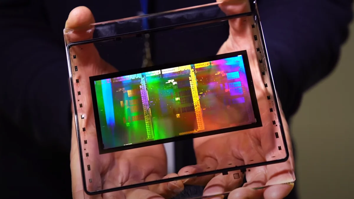
SANTA CLARA, Calif. — In a significant milestone for the resurgence of American semiconductor manufacturing, Intel Corporation announced on Wednesday that it has officially begun moving production equipment into its state-of-the-art Fab 62 facility in Arizona. The development marks a critical juncture in the company’s multi-year roadmap, keeping the facility firmly on schedule to achieve high-volume mass production by the late 2028 timeframe.
The announcement, delivered alongside broader updates regarding Intel’s expansive Ohio One manufacturing complex and its successful commercial integration of High-Numerical Aperture Extreme Ultraviolet (High-NA EUV) lithography, underscores the company’s aggressive pivot toward establishing a resilient, end-to-end domestic supply chain. Amid intense global competition and geopolitical pressures surrounding advanced electronics, Intel is positioning itself not merely as a fabricator of imported designs, but as the premier architect of homegrown semiconductor innovation.
Main Facts: The Scope of Intel’s Domestic Expansion
The latest operational updates from Intel Foundry highlight a multi-pronged strategy designed to secure American leadership in advanced microelectronics. The cornerstone of this week’s announcement is Fab 62, situated within Intel’s Ocotillo campus in Chandler, Arizona. With the arrival and initial rigging of complex manufacturing tools, the facility is transitioning from a massive construction project into an active, highly specialized cleanroom environment.
Concurrently, Intel provided updates on several other critical fronts:
- The Arizona Milestone: Fab 62 is tracking toward mass production by late 2028, where it will utilize Intel’s most advanced process nodes to serve both internal product divisions and external foundry customers.
- Ohio One Progress: Development continues at the massive Ohio One complex near Columbus, representing one of the largest single economic investments in the state’s history and a future hub for leading-edge silicon production in the American Midwest.
- High-NA EUV Integration: Intel confirmed that it has successfully integrated High-NA EUV lithography systems into high-volume manufacturing (HVM). This positions Intel as a pioneer in adopting the industry’s most advanced patterning technology, which is essential for printing ever-smaller features on silicon wafers.
- R&D and Packaging Ecosystem: Beyond front-end wafer fabrication, Intel is heavily investing in leading-edge process research and development, advanced 2D/3D packaging technologies, and domestic photomask production capabilities.
These initiatives are backed by a combination of private capital and public funding, most notably through the federal CHIPS and Science Act, which aims to restore domestic manufacturing capabilities for critical technologies.
Chronology: The Road to Fab 62 and High-NA EUV
To understand the weight of Wednesday’s announcement, it is necessary to examine the timeline of strategic decisions, construction milestones, and technological breakthroughs that have shaped Intel Foundry over the past several years.
The Foundation Years (2021–2022)
- March 2021: Newly appointed CEO Pat Gelsinger unveils the "IDM 2.0" strategy, outlining a massive pivot to open up Intel’s manufacturing network to external customers via Intel Foundry Services (IFS) while dramatically expanding internal capacity.
- March 2022: Intel announces an initial €33 billion investment package to boost manufacturing and R&D across Europe, alongside monumental domestic plans, including the announcement of the Ohio One mega-site and expansions in Arizona.
- September 2022: Construction crews break ground on major structural elements of the Arizona campus expansions, laying the physical groundwork for future facilities like Fab 62.
Technological Transition and Tooling (2023–2024)
- December 2023: Intel receives the world’s first commercial High-NA EUV lithography system (the ASML TWINSCAN EXE:5000) at its Ronler Acres campus in Hillsboro, Oregon, signaling the start of a multi-year effort to master sub-nanometer scaling.
- Throughout 2024: Construction progresses steadily at both the Arizona and Ohio sites despite macroeconomic headwinds. Intel refines its process roadmap, introducing nodes such as Intel 18A (1.8-nm class) designed to leverage backside power delivery and gate-all-around transistor architectures.
Execution and Operational Realization (Late 2025 and Beyond)
- Wednesday’s Announcement: Intel confirms the commencement of tool installation at Fab 62 in Arizona, officially anchoring the facility’s timeline to a late 2028 volume production target while validating the integration of High-NA EUV into real-world manufacturing flows.
Supporting Data: Infrastructure, Technology, and Capital
The sheer scale of Intel’s capital expenditure and technological deployment requires robust supporting infrastructure. Semiconductor manufacturing at the leading edge is arguably the most complex industrial endeavor on Earth, demanding microscopic precision, absolute environmental control, and unprecedented financial commitments.
The Economics of Leading-Edge Fabs
Building a modern leading-edge semiconductor fabrication facility requires investments ranging from $10 billion to over $20 billion per site. Fab 62 and the broader Arizona campus represent billions of dollars in specialized cleanroom space, chemical delivery systems, ultra-pure water recycling facilities, and power distribution networks.
Lithography and the High-NA Advantage
Lithography dictates how densely transistors can be packed onto a silicon wafer. Traditional EUV systems utilize a 13.5-nanometer wavelength of light. High-NA (High-Numerical Aperture) EUV systems increase the optical system’s numerical aperture from 0.33 to 0.55.
| Feature | Standard EUV (0.33 NA) | High-NA EUV (0.55 NA) |
|---|---|---|
| Numerical Aperture | 0.33 | 0.55 |
| Resolution Improvement | Baseline | ~1.7x denser feature printing in a single exposure |
| Manufacturing Impact | Requires multi-patterning for tightest pitches | Reduces mask steps, improving yield and cycle time |
By successfully integrating High-NA EUV into high-volume manufacturing, Intel aims to bypass the yield-robbing complexities of multi-patterning at sub-2nm nodes, granting the company a structural cost and performance advantage over competitors who are slower to adopt the technology.
The Packaging and Photomask Pillar
Manufacturing the raw silicon wafer is only half the battle. Modern computing relies heavily on advanced packaging—such as Intel’s EMIB (Embedded Multi-Die Interconnect Bridge) and Foveros technologies—which allow multiple chiplets to be stitched together into a single, cohesive processor. By investing concurrently in U.S.-based advanced packaging and photomask fabrication, Intel ensures that the entire lifecycle of a chip—from design layout to final encapsulated package—can be secured domestically.
Official Responses: Defining "American-Made"
The strategic rationale behind Intel’s massive capital allocation was forcefully articulated by company leadership on Wednesday. In a public statement addressing the philosophical and practical differences in semiconductor sourcing, Naga Chandrasekaran, executive vice president and chief technology and operations officer for Intel Foundry, drew a sharp line between assembly and true domestic innovation.
"There is an important difference between technologies made in America and technologies that are truly American-made," wrote Chandrasekaran. "The difference lies in the research and development process that transforms ideas into manufacturable technologies."
Chandrasekaran’s remarks strike at the heart of modern global electronics supply chains. While various entities can package or test imported silicon within U.S. borders—qualifying as "made in America" under certain regulatory definitions—Intel argues that authentic technological sovereignty requires owning the foundational R&D, the process engineering breakthroughs, and the core intellectual property generation on domestic soil.
Industry analysts have noted that this perspective reinforces Intel’s unique value proposition as an American-headquartered foundry that controls the entire stack from silicon design rules to physical fabrication and packaging.
Implications: Geopolitics, Competition, and the Future of Compute
The ramifications of Intel’s operational progress at Fab 62, Ohio One, and its R&D labs extend far beyond corporate balance sheets. They touch upon national security, global economic stability, and the future trajectory of the computing industry.
1. National Security and Supply Chain Resilience
For decades, the global semiconductor supply chain has suffered from extreme geographic concentration, with the vast majority of the world’s most advanced processors manufactured within a few square miles in East Asia. By establishing redundant, advanced manufacturing nodes in Arizona and Ohio, the United States takes a monumental step toward mitigating single-point-of-failure vulnerabilities that could be triggered by geopolitical conflict, natural disasters, or public health crises.
2. Competitive Positioning in the Foundry Market
Intel Foundry is locked in a fierce multi-company race against established pure-play foundries like TSMC and Samsung Electronics. By integrating High-NA EUV ahead of broad industry adoption and maintaining a robust domestic footprint, Intel aims to prove to fabless designers—such as Qualcomm, NVIDIA, AMD, and hyperscale cloud providers—that it is a reliable, technologically competitive alternative for outsourcing next-generation silicon.
3. Economic Impact and Workforce Development
The multi-billion-dollar investments in Arizona and Ohio are creating tens of thousands of high-paying jobs, ranging from construction workers and facilities engineers to chemical technicians and PhD-level process scientists. Furthermore, Intel has partnered extensively with community colleges and major universities to establish specialized curricula, ensuring that the American workforce possesses the specialized skills required to operate the world’s most advanced manufacturing facilities.
Looking Ahead to 2028
As production tools hum to life inside Fab 62, the countdown to late 2028 has officially begun. While the road ahead involves overcoming immense technical hurdles inherent in sub-nanometer scaling, Intel’s systematic execution of its tool-in milestones demonstrates that the vision of a self-sustaining, cutting-edge American semiconductor ecosystem is steadily moving from blueprint to reality.

