

Main Facts
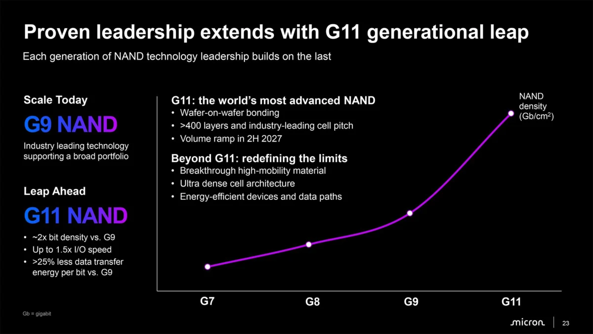
Semiconductor giant Micron Technology has detailed its ambitious technological roadmap for its next-generation 3D NAND flash memory architecture, slated to enter commercial mass production in the second half of 2027. Revealed during a high-profile corporate briefing this week, the upcoming flash memory memory generation promises a radical transformation in non-volatile storage capabilities.
According to Micron’s engineering disclosures, the upcoming 3D NAND platform will deliver three transformative performance and efficiency pillars:
- A 100% Increase in Storage Density: Doubling the overall capacity per square millimeter compared to the company’s current-generation production nodes.
- A 50% Boost in I/O Performance: Significantly accelerating data transfer rates relative to existing commercialized NAND products.
- Substantial Power Reductions: Lowering active and idle energy consumption profiles to meet the stringent power demands of modern hyperscale data centers, edge artificial intelligence (AI) devices, and mobile computing.
To achieve these aggressive metrics, Micron is pivoting its manufacturing strategy, most notably by adopting wafer-on-wafer (WoW) hybrid bonding—a technique pioneered and popularized by industry rivals such as Yangtze Memory Technologies Corp (YMTC). Beyond the 2027 deployment, Micron’s research and development (R&D) teams are already exploring novel materials and ultra-dense memory cell architectures designed to push 3D NAND vertical and horizontal scaling well beyond the forthcoming Generation 11 (G11) node.
Chronology
The path to Micron’s 2027 3D NAND paradigm shift is built upon a multi-year evolutionary timeline of architectural transitions, manufacturing milestones, and competitive adaptations.
The Foundation: The Replacement Gate Era (2020–2022)
For years, the flash memory industry relied on floating-gate technology to store electrical charges. However, as vertical scaling surpassed 100 layers, floating-gate interference became a critical bottleneck. Micron transitioned decisively to a Replacement Gate (RG) architecture, culminating in its 128-layer node. This shift allowed the company to scale cell density more predictably while controlling manufacturing complexity.
The 232-Layer Breakthrough (2022–2023)
In late 2022, Micron disrupted the memory market by shipping the world’s first 232-layer 3D NAND flash memory. Manufactured primarily at its facility in Singapore, this node utilized a dual-deck architecture to stack strings of memory cells vertically. It established Micron as a technological leader in raw layer count and areal density, outperforming several legacy competitors who remained mired in lower-layer designs.
The Pivot to CMOS-Under-Array (CUA) and G9 (2023–2025)
As vertical scaling approached physical limits, Micron focused heavily on peripheral circuit placement. By shifting the CMOS logic circuitry from beside the memory array to directly underneath it (CMOS-Under-Array or CUA), Micron reclaimed valuable silicon real estate. This era set the stage for the development of Generation 9 (G9) and Generation 10 nodes, steadily creeping toward higher yields and faster interface speeds.
The Strategic Shift to Wafer-on-Wafer Bonding (2025–2027)
Recognizing that traditional manufacturing limits were restricting further performance gains, Micron’s internal roadmap underwent a strategic recalibration. Observing the commercial success of YMTC’s Xtacking technology—which bonds a dedicated CMOS wafer to a dedicated memory array wafer independently—Micron decided to integrate wafer-on-wafer hybrid bonding into its 2027 generation. This move represents a departure from single-wafer sequential processing toward a modular, dual-wafer manufacturing paradigm.
Supporting Data
The technological metrics released by Micron underscore the scale of the engineering challenges the company is attempting to overcome, as well as the magnitude of the performance leap expected in 2027.
| Metric / Feature | Current-Gen Micron NAND | Next-Gen 3D NAND (Target: 2H 2027) |
|---|---|---|
| Storage Density | Baseline (1x) | 2x (Doubled capacity per die) |
| I/O Performance | Baseline (e.g., 2,400–3,200 MT/s) | +50% Increase |
| Power Efficiency | Standard operational draw | Significantly Decreased (Lower mW/GB) |
| Bonding Technology | CMOS-Under-Array (CUA) | Wafer-on-Wafer (WoW) Hybrid Bonding |
| Target Era | Current Production (G9/G10) | Post-G11 / Advanced Scaling |
Analyzing the 50% I/O Performance Surge
Modern enterprise solid-state drives (SSDs) and client storage solutions are increasingly bottlenecked not by raw NAND read/write endurance, but by the speed at which data can be transferred across the bus between the NAND flash chips and the SSD controller. By engineering a 50% increase in I/O performance, Micron aims to clear a major hurdle for PCIe 6.0 and future interface standards. This will allow sustained sequential throughputs to scale beyond current ceilings without requiring wider, more complex physical data channels.
The Mechanics of Wafer-on-Wafer (WoW) Bonding
In a conventional monolithic 3D NAND manufacturing process, peripheral logic circuits and the memory cell array are fabricated sequentially on the exact same piece of silicon. This introduces severe design compromises: the thermal budgets and processing steps required for memory arrays can degrade CMOS logic performance, and vice versa.
With wafer-on-wafer hybrid bonding, Micron will process the memory array on one silicon wafer and the high-performance CMOS logic circuitry on a completely separate wafer. The two wafers are then meticulously aligned and fused together at the atomic level using copper-to-copper direct bonding.
- Independent Optimization: The memory array can be optimized exclusively for maximum vertical layer density and electron trapping efficiency.
- Advanced Logic: The peripheral CMOS circuit can be manufactured on a more advanced logic process node, yielding faster decoders, error-correction engines, and interface drivers.
- Die Size Reduction: Because the logic sits underneath or across the bonded plane without sharing footprint constraints, overall die size shrinks, improving wafer yield economics.
Official Responses
Micron’s executive leadership and principal engineering teams have framed this forthcoming architecture not merely as a routine product refresh, but as a structural reimagining of how non-volatile memory will support the data-intensive computing landscape of the late 2020s and beyond.
During the company’s recent strategic briefing, Micron’s executive vice president of technology development emphasized that the memory industry has crossed a threshold where brute-force vertical stacking alone is no longer economically or physically viable.
"Scaling 3D NAND into the latter half of this decade requires us to rethink our foundational toolset," noted a senior Micron engineering representative during the briefing. "By embracing wafer-on-wafer hybrid bonding, we are breaking free from the traditional constraints of monolithic processing. We can now scale our memory arrays and our CMOS logic independently, unlocking performance tiers—specifically a 50% jump in I/O speeds and a doubling of density—that would otherwise remain out of reach."
Industry analysts present at the briefing noted that Micron’s open acknowledgment of adopting wafer-on-wafer techniques—historically pioneered by YMTC and heavily guarded by various international patents—signals a pragmatic shift in the competitive landscape. Rather than avoiding architectural designs popularized by competitors, Micron is validating the effectiveness of hybrid bonding as the definitive path forward for high-density flash memory.
Furthermore, corporate communications highlighted that the reduction in power consumption is a direct response to global sustainability initiatives and the soaring energy costs associated with artificial intelligence data centers. As hyperscalers demand denser storage footprints that do not exponentially increase thermal output, Micron’s next-generation architecture is positioned as a direct solution to the cooling and power delivery crises facing modern server farms.
Implications
The introduction of Micron’s advanced 3D NAND architecture in 2H 2027 carries profound implications for the global semiconductor supply chain, enterprise IT infrastructure, consumer electronics markets, and the geopolitical landscape of memory manufacturing.
1. Enterprise Storage and Hyperscale Data Centers
The exponential growth of generative AI training models, large language models (LLMs), and big data analytics has placed unprecedented pressure on enterprise storage hierarchies.
- TCO Reduction: Doubling storage density means data centers can rack twice the amount of raw flash capacity within the exact same rack space, drastically lowering Total Cost of Ownership (TCO).
- Latency Mitigation: The 50% increase in I/O performance helps bridge the gap between high-speed DRAM and persistent storage, reducing query latencies for data-intensive retrieval-augmented generation (RAG) AI workloads.
2. Client Devices and Mobile Computing
For everyday laptops, smartphones, and edge-computing devices, Micron’s breakthroughs translate to longer battery life and higher capacity configurations at lower price points.
- Thermal and Energy Efficiency: Lower power consumption in NAND flash chips directly extends battery longevity in thin-and-light laptops and mobile handsets, while mitigating the thermal throttling issues that plague high-performance NVMe SSDs in compact chassis.
- Massive Local Storage: As mobile applications, on-device AI models, and high-resolution media capture demand larger storage footprints, the ability to double density on silicon wafers ensures that 4TB and 8TB capacities will become economically viable in mainstream client form factors.
3. Competitive Dynamics and Patent Landscapes
Micron’s strategic pivot to wafer-on-wafer bonding alters the competitive dynamics between major flash memory producers, which include Samsung Electronics, SK Hynix, Kioxia, Western Digital, and YMTC.
- Validation of Hybrid Bonding: For years, wafer-on-wafer and similar hybrid bonding methodologies were viewed with skepticism by some western and east-Asian manufacturers due to alignment tolerances, yield risks, and intellectual property complexities. Micron’s public commitment normalizes hybrid bonding as the industry-standard methodology for post-G11 3D NAND.
- Pressure on Competitors: Samsung and SK Hynix, who have historically relied on alternative peripheral-under-cell (Peri-Under-Cell or PUC) variations of monolithic integration, may be forced to accelerate their own hybrid bonding roadmaps to match Micron’s projected density and I/O advantages.
4. Long-Term R&D and Beyond-G11 Horizons
Looking past Generation 11, Micron’s disclosure that it is actively developing new materials and denser memory cell architectures indicates that the roadmap does not stop at wafer bonding. As traditional silicon oxide/nitride dielectrics face electron leakage and physical thinning limits, the integration of novel trap materials—potentially moving toward ferroelectric or transition metal dichalcogenide (TMD) variants—will be necessary. Micron’s aggressive R&D posture ensures that flash memory will continue to scale well into the 2030s, preserving Moore’s Law-equivalent scaling trajectories in non-volatile solid-state storage.

